
Packaging keeps its cool
Packaging innovation leads to vastly improved cooling and thermal management, says Stefan Preimel, concept and application engineer, Infineon Technologies
Packaging innovation leads to vastly improved cooling and thermal management, saysn order to meet the common goals of modern SMPS design, including fast switching, high efficiency, reduced size and weight and minimised total cost of ownership, semiconductor materials have been the subject of significant development activity. By driving down on state resistance, improving gate charge and reducing switching losses, the latest super-junction MOSFET technologies in combination with the improved CoolSiC Schottky diode technologies address these challenges in modern hard- and soft-switching applications.
Until relatively recently, the most common packages used for power switching devices were through-hole types such as TO-220 and TO-247. Their long leads however lead to parasitic inductance that reduces switching speeds, meaning that associated magnetic components are larger and more expensive. They also require a special process step to fit them into the PCB and solder them, increasing production complexity and cost.
SMDs have shorter leads and are easier to handle in production, but are generally cooled by contact with the PCB, either through their body or the component leads. This remains one of the major challenges for applications such as power factor correction (PFC) circuits, and is the main reason that TO-220 and TO-247 remain the most common package types used for high power SMPS applications.
Turning cooling upside down
The Double DPAK (DDPAK) package from Infineon Technologies is a surface mountable package for power devices that delivers top-side cooling (Conventional SMD packages disperse heat down into the PCB.) The concept is optimised for high power, high voltage and high reliability applications and is suitable for both MOSFETs and SiC diodes (Figure 1).
 package by Infineon Te.._.png) Figure 1: DDPAK technology incorporates top-side cooling in an SMD package
Figure 1: DDPAK technology incorporates top-side cooling in an SMD package
The DDPAK offers five connections for the drain current, three source connections and one source sense connection for the gate reference potential, as well as a single connection for the standard gate drive. This four-pin approach is possible with conventional through-hole packages and would allow for electrically cleaner driving signals that reduce switching losses in the application, but space constraints remain an issue.
The DDPAK is smaller than the TO-220 package, saving space and allowing greater power densities, and has an 18% improvement in thermal coupling between the semiconductor junction and the case. The form factor also allows for thinner end products to be designed.
Many product safety standards stipulate the maximum temperature that a FR4-based PCB can reach during operation. When the semiconductor device is in direct contact with the PCB this rule limits the temperature of the semiconductor.
Making contacts
One challenge with conventional SMD packages that are mounted on PCBs is the different rate of thermal expansion of the device/package and the PCB itself, due to the different co-efficients of thermal expansion (CTE) of the two materials. The temperature cycling on board (TCOB) test is defined by IPC9701 to address this issue.
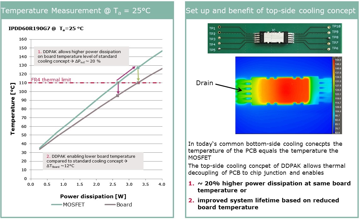
Figure 2: Separating the DDPAK from the PCB overcomes challenges associated with conventional SMD packages
The leads on a DDPAK have a spring-like quality and act as a buffer between the body and the PCB. This eliminates CTE-related failure modes including solder joint fatigue and internal package defects due to the stress. When a TCOB test with over 2000 cycles was performed on a DDPAK there were no failures.
For almost all practical applications some form of heatsinking is required to be attached to the top-side to assist the movement of thermal energy away from the semiconductor junction and into the ambient surroundings. Options for affixing the heatsink to the package include the use of clips, push pins, adhesives or direct soldering.
The company believes that DDPAK brings a new packaging concept that meets the needs of even the most demanding applications. When combined with the latest Infineon silicon technologies, such as CoolMOS G7 and CoolSiC G6, Infineon believes it delivers a significant step forward in switching devices for market-leading SMPS.
Visit Infineon at PCIM 2018
Hall 9 - 412
Product Spotlight
APV1111GVY
Panasonic

Panasonic PhotoMOS® Photovoltaic MOSFET High-Power Drivers
| SKU: | |
|---|---|
| Stock: | 3490 |
| Cost: | $3.95 |
