
Minimising EMI in power supply designs
Designing to minimise EMI is less difficult when the problem is addressed correctly, following standard practices and using proven techniques, even in power supply design. By Shane Callanan, Director of Applications Engineering, Excelsys Technologies.
EMI is everywhere; nature provides many sources of electromagnetic interference and the sun is a major source of radiation on a daily basis. However, for electrical equipment we usually only have to deal with man-made sources of radiation. These can be intentional such as radio, TV, telephony and other RF signals, or they can be unintentional; sources that appear as as result of load distribution, vehicle ignition systems and even power supplies.
Any source of changing voltage or changing current with respect to time will result in ringing, and any given switch mode power supply will be full of these events occurring every switching cycle. All tracks, points and components are a potential source of this on a power supply, but the hidden truth is that most EMC sources do not appear on any bill of materials. Within any given design there will be loops with high di/dt and high dv/dt’s. Figure 1 identifies the potential areas for high di/dt’s in an isolated forward converter, while Figure 2 shows the potential areas for high dv/dt’s in the same design.
With such high di/dt’s and dv/dt’s it doesn’t take much interwinding capacitance to generate significant common mode currents and voltage spikes of up to several volts. This will result in ground bounce, and hence EMI. If we continue with this path of investigation we can also look at the example of a FET going from a Vds of 200V in 40nS. This equates to a dv/dt of 5 billion volts per second!
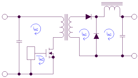
Figure 1 - High di/dt loops on a forward converter
Designing power supplies for good EMI performance is not a black magic. With the correct knowledge and experience, limiting EMI can be accommodated right from the project concept stage. This includes a heavy focus on the design and layout of the PCB, as this will play a significant role in emissions. The first focus for any designer is to eliminate or at least minimise the emissions from the source of the generators. Also remember that receivers re-transmit, so minimise the susceptibility of receivers. If this is still not achieving the target emissions then as a final solution you may need to look at filters, but it should be remembered that filters can require significant additional space in a final design.
PCB layout plays it part
PCB layout is often the least understood factor when designing for EMI, but it need not be difficult if the following points are observed: minimise loop areas; leave no floating parts, ensuring that all loops are brought back to ground, and; keep signal and power ground connections separate.
This will add to the complexity of the PCB design so there are normal compromises in order to save on layers. On one layer you should track the input and output signal grounds with the star points at the IC’s common pins (allow for the isolation barrier between input and output). On a separate layer the ground plane for the power grounds. Input ground plane under the input components only, output ground plane under the output components only, allow for the isolation barrier between input and output ground planes. Also, remember that earthing schemes were designed for safety purposes, not EMI, so use ground planes and short connections. Also there should be only one connection between signal and power grounds, through a via at the signal ground star point.
The difficulty facing power supply designers is that EMI performance is not usually characterised by the component manufacturer. Understanding your components is key to knowing how they will behave in terms of emissions. This is especially true at the highest effective frequency. You must also consider that things like capacitors, wire wound resistors and even wire leads will vary in behaviour as the frequency changes. This also holds true for the type of capacitors used, as tantalum capacitors behave differently to, say, ceramic capacitors. Your parasitic components, ESR, ESL, Cs and leakage will all play their part, so knowing and quantifying these are all key to understanding EMI. Most EMC components are invisible on the circuit diagram as are either stray and parasitic components; everything must be done with sound RF principles in mind.
Compliance of the power supply in a test house to various limits does not necessarily guarantee the user that it will pass when installed into a system. There are a number of causes of poor system noise performance, including: insufficient de-coupling on the PCB or load; faulty wiring connection or poor cable terminations, or poor system earthing. There are also some simple steps to eliminate, reduce or identify the causes of high frequency noise; is the noise conducted or radiated? If changing the position of the power supply or screening improves performance, the noise is likely to be radiated. Twist all pairs of power and sense cables separately, and Ground connections (zero Volt) should be made to the nearest point on the chassis.
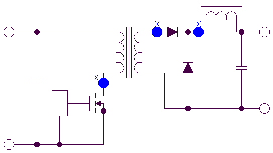
Figure 2 - High dv/dt areas on a forward converter
In the same way that the power supply designer needs to ensure that the sources for radiation are kept to a minimum, the system designer also has a role to play in ensuring that the overall system has the optimum performance. Cabling arrangements and PCB tracking layouts are the greatest contributing factor to system EMC performance. It is important that PCB tracks and power cables are arranged to minimise current carrying loops - which can radiate - and to minimise loops that could have noise currents induced into them. All cables and PCB tracks should be treated as radiation sources and antennae, and every effort should be made to minimise their interaction.
In general, keep all cable lengths as short as possible, and minimise the area of power carrying loops to minimise radiation, run PCB power tracks back to back and minimise noise current induced in power or signal carrying lines, by using twisted pairs for cables with the maximum twist possible. Also, do not combine power and sense cables in the same harness, and ensure a good system ground. System Earth should be a ‘starpoint’, and input earth of the equipment should be directed to the starpoint as soon as possible. The power supply earth should be connected directly to the starpoint; all other earths should also go to the starpoint.
Electro Magnetic Interference is considered by many as being a black art, but the truth of the matter is that with sufficient knowledge, due diligence and attention to detail you can design your power supply to have the optimum performance. Trying to address this issue at the back end of a design process can be costly, time consuming and end up having to use relatively large filters. Power supplies by their nature are noisy environments, but taking every aspect of the design into consideration a market leading performance is achievable. Reduce your common mode impedances, know your components, and layout your PCB correctly at the beginning of your design cycle. This will minimise your troubleshooting EMI problems later. Above all remember that EMI design is the sum of many small items, and only when all of these are addressed will you see improvements in the emissions.
Product Spotlight
APV1111GVY
Panasonic

Panasonic PhotoMOS® Photovoltaic MOSFET High-Power Drivers
| SKU: | |
|---|---|
| Stock: | 3490 |
| Cost: | $3.95 |
