ICs slash BoM with integrated feedback circuits
By integrating primary and secondary feedback circuits, the InnoSwitch IC family is set to revolutionise switch-mode power supply design, says Power Integrations. The ICs use FluxLink safety-isolated communication technology, which combines primary - and secondary-switcher circuitry to reduce component count.
There is no need for optocouplers, says the company, and it claims that the ICs outperform primary-side controllers.
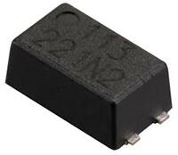
Inside the surface-mount package, the secondary-side direct voltage and current measurements are communicated across the safety isolation barrier via high-speed digital FluxLink technology. The proprietary feedback technique allows control, but without the limited accuracy and efficiency of primary-side regulation or the poor transient response of no-load consumption.
The ICs include a high-voltage power MOSFET, primary-side controller, FluxLink feedback technology and a secondary-side controller with synchronous rectification. Combining synchronous rectification with the secondary-side master controller, and communicating across the fast FluxLink channel, maximises synchronous rectification switch timing. The fast communication link also eliminates shoot-through in either discontinuous conduction mode or continuous conduction mode, even during transient loads and fault conditions. This synchronous rectification performance in both DCM and CCM modes is an advantage in adaptive- voltage charger applications. (The ICs are already in chargers from two of the world’s leading mobile device makers.)
InnoSwitch ICs start up using bias current drawn from a high-voltage current source connected to the drain pin, eliminates the need for external start-up components. An external bias winding reduces no-load and increases system efficiency during normal operation.
The ICs also include system-level features such as output over-voltage protection, overload power limiting, hysteretic thermal protection and frequency jitter to reduce EMI. The company says that, unlike primary-side regulated switchers, the InnoSwitch-based, secondary-side regulated designs are less sensitive to the tolerance of external components such as transformers, diodes, resistors and capacitors. This increases manufacturing yield and reduces total power supply cost. This is illustrated with the example of mobile device chargers which can have up to 5A and the component count of a primary side regulated design, with CV and CC control of (±3 and ± 5% respectively) and low voltage ripple. With high operating efficiency and less than 10mW no-load consumption, the ICs comply with efficiency standards such as the California Energy Commission, European Union Code of Conduct (CoC) Version 5, Tier 2, and the US DoE standards, which will be mandatory in February.


