Changing markets are served by gate driver ICs
Energy-savings has become essential in equipment’s design. Therefore, high efficiency of inverter and converter circuits used in power electronics, especially for power supply and motor drives requiring high-power conversion, has become indispensable.
By Raimund Wagner, Rohm Semiconductor.
In recent years, attention is focused on power electronics, mainly in the fields of industrial equipment, renewable energy and automotive-inverters. In the field of industrial equipment, factory automation and robotics have progressed, and markets for general-purpose inverters/UPS and servo amplifiers have been expanding year after year. New markets are emerging for power converters, including solar-inverters and power-storage devices in the field of renewable energy and for EV/HEV in the automotive field.

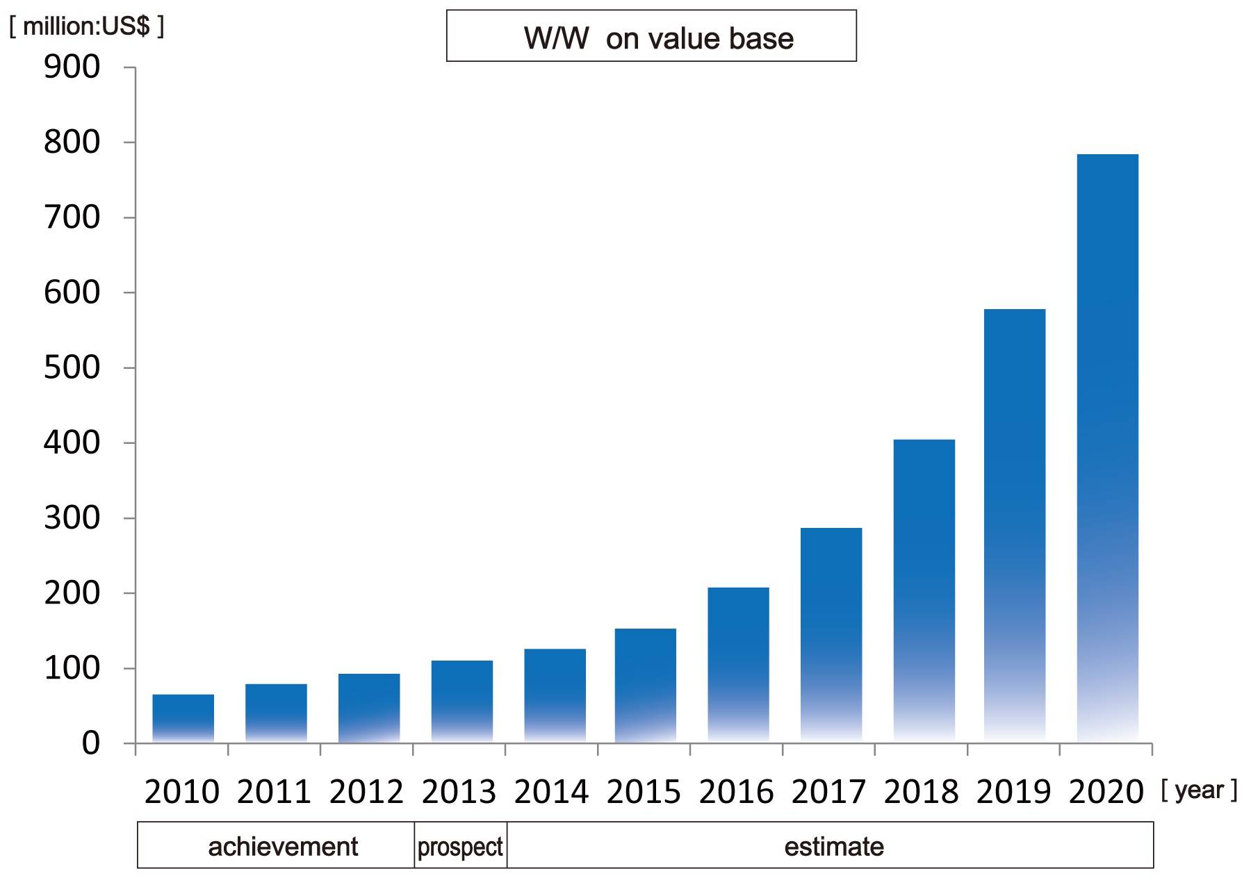
Figure 1: Market trend of SiC power devices using data compiled by Rohm, based on Fuji Keizai Reality and Future Prospect of Next Generation Power Device and Power Electronics Related Apparatus Market 2013
In Europe, recent developments include design-upgrades to improve efficiency by using high-frequency circuits for solar-inverters, high-power UPS, cellular basestation power supplies, fuel-cell systems and railway power converters, which demands gate drivers with isolators.
While high efficiency is required, challenges for downsizing have also increased. This is generally attained by high frequency operation that requires optimising gate drive voltage for the SiC MOSFET, IGBT and power-MOSFET devices. The effect of surges and influence of switching-noise has to be considered as voltage increases.
Inverter applications
Market expansion is expected for SiC power devices, which are progressively adopted in next-generation inverters, as keystones for high efficiency. Adoption of SiC-diodes has already started implementing in PFC circuits of high-capacity power supplies and power-conditioners, and take up of products using SiC MOSFET for switching applications is expected to increase gradually in the future.
While SiC MOSFETs make inverters highly efficient by high-speed switching, there are problems similar to those of conventional power devices such as counter-measures against the noise generated in gate drive circuit and safe design of protection circuits at the time of abnormality, such as short circuit.
Under these circumstances, gate driver circuits adopted with conventional photo-coupler system for power devices such as SiC and IGBT are indispensable in the field of medium/high voltage and high power applications. However, inferior high-temperature property and low speed of photo-coupler plague SiC circuits, whose advantage is in high-speed switching. Rohm developed gate drivers with built-in isolators that can maximise performances of SiC, IGBT and power MOSFET using built-in isolators inside the ICs. The BM6104FV has built-in short-circuit protection; the BM60014FV has a simpler construction to advance product development quickly, to meet market needs.
The gate drivers realised compact packages by combining its original Bi-CDMOS technology with newly developed On-chip transformer technology. This uses two embedded copper coils which are separated by a Silicon-Oxide layer as an isolator. The thickness of this layer defines the level of isolation. The inductive coupling method uses a changing magnetic field between the two coils to realise the communication across the isolation layer. The advantage of inductive coupling is the flexibility of the structure. With careful transformer design it is possible to achieve high common-mode impedance to the noise and low differential impedance to the signal for high switching speeds. The signal energy transfer can be nearly 100%, which makes it possible to design very low-power isolators. Optimising the design of the isolator minimises the influence of external magnetic fields.
Isolator technology
This isolator technology is used with a low voltage interface chip and a high voltage gate driver chip within a compact multi-chip IC package. The BM6104FV mounting-area was reduced by about 50% compared to conventional photo-coupler circuits. A compact IC package also contributes to downsizing of inverter and converter circuits. The number of parts is reduced with the built-in isolator IC, and also improves inverter-circuit reliability and downsizes drive substrates.
The optimisation of the isolator as well as the interface and gate driver reduces the I/O delay-time to less than half that of the first-generation products to realise high speed.
SiC MOSFET still has problems similar to those of conventional power devices, i.e. countermeasures against the noise generated in gate drive circuit, and safe design of protection circuits at the time of abnormality, such as a short circuit.
To reduce power consumption the gate driver assesses abnormality when a short-circuit occurs by means of the output short-circuit protection function. It stops switching and, at the same time, activates ‘soft turn-off’. This enables safe control of inverter action even during abnormality. Integrating protection functions contributes to the downsizing of inverters as well as the reduction of design load.
MOSFET SiC
MOSFET using SiC (Silicon Carbide) is expected to be the next-generation power semiconductor, with the ability to realise high-efficiency, low power-consumption in high-power inverters and next-generation EVs.
Rohm’s original core-less transformer technology with integrated isolation function realises a compact package. The SSOP-B20W measures 6.5x8.1x2.01mm max, to reduce mounting area by over 50% compared with conventional package types.
All protection functions required for inverter circuits are built-in, including mirror-clamp function, fault-output function, under-voltage lock-out function, short-circuit protection function, and soft turn-off. Gate state monitoring function is also integral in the BM6104FV.
I/O time is high at 150ns. Delay-time was reduced to less than half from conventional products. A minimum I/O pulse width of 90ns was also realised. The operating temperature range is -40 to +125°C. A small variation of delay time in a wide temperature range makes it easy to examine a drive circuit design. It can also correspond to automotive inverters in severe temperature environment.
PCIM 2015: Hall 9 - 316


