
Build high energy density power supplies with integrated eGaN
High energy density switch-mode power supplies (SMPSs) can accelerate battery charging, reduce the size of solar micro-inverters, and meet the demand of server farm power requirements, all without generating excessive heat. However, engineers are now reaching the performance limits of the silicon MOSFETs and IGBTs that form the primary switching elements of conventional SMPSs. Instead, transistors constructed from enhancement-mode gallium nitride (eGaN)—a wide bandgap semiconductor—can now be used to overcome the switching speed and efficiency limitations of silicon devices.
Previously, the cost and availability of eGaN transistors precluded their use in anything but the most esoteric power supply applications, but wider commercialisation has resolved those challenges. eGaN transistors are now an option for a much wider range of applications.
In this article Rich Miron, Applications Engineer at Digi-Key Electronics describes the advantages of high frequency power supplies based on eGaN switching components compared to those based on conventional silicon (Si) MOSFETs or IGBTs. He then presents guidelines on how to build SMPS designs suitable for applications such as battery charging or server farms using eGaN power stages from EPC, Texas Instruments, and Navitas Semiconductor.
High frequency benefits
Conventional SMPSs typically employ switching frequencies ranging from tens to hundreds of kilohertz (kHz). The duty cycle of the pulse width modulation (PWM) of the base frequency determines the power supply’s voltage output.
The key benefit of a higher switching frequency is a reduction in the size of peripheral components such as inductors, transformers, and resistors. This allows a designer to shrink designs for the same output power, increasing the energy density. In addition, current and voltage ripple at the SMPS output is reduced, lowering the risk of electromagnetic interference (EMI) as well as the cost and size of filter circuits.
However, conventional silicon power MOSFETs and IGBTs switch relatively slowly and dissipate significant power each time the devices switch on and off. Those losses multiply as the frequency increases, reducing efficiency and raising chip temperatures. The combination of slow switching and high switching losses puts a ceiling on the practical switching frequency of today’s SMPSs.
Designers can break this ceiling by turning to wide bandgap semiconductors. Of these, GaN is currently the most proven and accessible technology for this application, with eGaN being a more refined version of GaN.
Comparing silicon with GaN
GaN offers several advantages over silicon, including several related to the material’s higher electron mobility. Increased electron mobility bestows the semiconductor with a higher breakdown voltage (above 600 volts) and superior “current density” (amperes/centimeter2(A/cm2)). Another advantage of GaN is that transistors constructed from the material don’t exhibit reverse recovery charge, a phenomenon that can lead to high switch current overshoot (ringing).
But while these characteristics are important to the power supply designer, perhaps more critical is that high electron mobility allows a GaN transistor to switch in about one quarter of the time of a silicon MOSFET. Additionally, each time the GaN device switches, losses are around 10 to 30 percent those of a silicon transistor for a given switching frequency and current. As a result, GaN high electron mobility transistors (HEMTs) can be driven at much higher frequencies than silicon MOSFETs, IGBTs, or silicon carbide (SiC) devices (Figure 1).

Figure 1: GaN HEMTs enable higher frequency switch-mode power supplies than do silicon or SiC devices. (Image source: Infineon)
GaN HEMTs have been slow to catch on for two key reasons. First, the devices are essentially depletion mode field-effect transistors (FETs), so the default mode is “on”. In contrast, silicon MOSFETs are enhancement mode devices with an “off” default mode. Consequently, GaN HEMTs require the addition of carefully tuned bias networks for proper operation. Second, the transistors are fabricated using a different process than the mature, high-volume techniques used for silicon, making them more expensive. This design complexity and higher cost has limited GaN HEMT applications to high-end SMPSs.
But recently, eGaN HEMTs have been commercialised and are eliminating the need for bias networks. Moreover, chip vendors have introduced integrated power ICs drivers based on eGaN HEMTs that simplify design. Also, increased production levels have enabled lower cost eGaN devices.
Integrated GaN solutions
In high-end SMPS designs where eGaN HEMTs were previously used, the high price forced designers to limit the devices’ use to power transistors, and then revert to silicon MOSFETs for the gate drivers. While some performance gains were achieved compared to “all silicon” designs, the silicon elements in the combined design compromised maximum switching frequency. Also, because GaN and silicon use different process technology, the gate driver and power transistors had to be fabricated as separate components, increasing cost and pc board footprint.
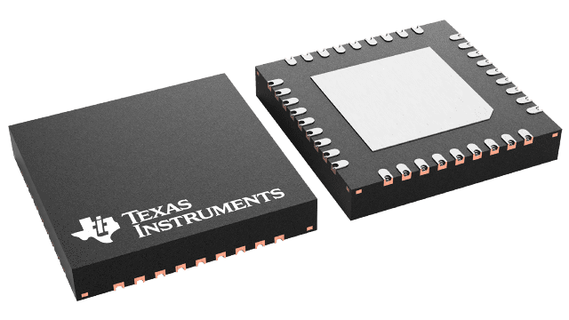
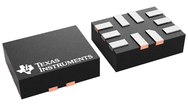
Lower eGaN prices have allowed chip makers to address both problems. Texas Instruments, for example, offers its LMG3411R070 70 milliohm (mΩ), 600 volt eGaN power stage with integrated gate driver (Figure 2).

Figure 2: The LMG3411R070 from Texas Instruments integrates a 70 mΩ, 600 volt eGaN power stage with its driver. (Image source: Texas Instruments)
The chip can switch 100 volts/nanosecond (ns) with near zero ringing (Figure 3). This compares with typical slew rates of 3 to 10 volts/ns for conventional silicon power MOSFETs.

Figure 3: As demonstrated by TI’s LMG3411R070 integrated eGaN power stage, eGaN power transistors can manage much higher slew rates than MOSFETs with minimal ringing. (Image source: Texas Instruments)
Navitas Semiconductor manufactures a similar class of product, the NV6113. The product integrates a 300 mΩ, 650 volt eGaN HEMT, a gate driver, and associated logic in a 5 x 6 millimeter (mm) QFN package. The NV6113 can withstand a slew rate of 200 volts/ns and operates at up to 2 megahertz (MHz).
While devices such as the TI and Navitas GaN power stages can be deployed in parallel for use in the popular half-bridge topology (Figure 4), other products are available that integrate two power transistors (and associated gate drivers) on the same chip.

Figure 4: The Navitas NV6113 can be deployed in parallel for half-bridge topologies as shown here. (Image source: Navitas Semiconductor)
EPC, for example, recently introduced its EPC2115, an integrated driver IC that comprises two monolithic 88 mΩ, 150 volt eGaN power transistors, each with an optimised gate driver (Figure 5). The EPC2115 comes in a low inductance, 2.9 x 1.1 mm BGA package and can run at up to 7 MHz.

Figure 5: EPC’s eGaN integrated driver IC includes two power transistors, each with its own optimised gate driver. (Image source: EPC)
Designing a power supply using eGaN HEMTs generally follows the same principles as a design using silicon MOSFETs, but the higher operating frequency impacts peripheral component selection.
Peripheral component selection
To illustrate the impact of frequency on component selection, consider the input capacitor for a simple DC-to-DC SMPS step-down (“buck”) topology.
Input capacitors reduce input ripple voltage amplitude, and in turn dampen ripple current to a level that can be handled by relatively inexpensive bulk capacitors without excessive power dissipation. Reducing peak-to-peak voltage ripple amplitude to below 75 millivolts (mV) is a good rule of thumb for keeping the currents in the bulk capacitors within acceptable limits. The input capacitor is typically a ceramic device because they have the extremely low equivalent series resistance (ESR) needed to effectively reduce voltage ripple.
To determine the value of the ceramic input capacitor needed to reduce peak-to-peak voltage ripple amplitude to a given magnitude, Equation 1 can be used:
![]()
Where:
- CMIN is the minimum required ceramic input capacitance in microfarads (μF)
- fSW is the switching frequency in kHz
- VP(max) is the maximum allowed peak-to-peak ripple voltage
- IOUT is the steady state output load current
- dc is the duty cycle (as defined above)
- (From Reference 1)
Performing the calculation with some typical operational values for a high-end silicon-based power stage yields:
- VIN = 12 volts
- VOUT = 3.3 volts
- IOUT = 10 A
- η = 93 percent
- fSW = 300 kHz
- dc = 0.296
- VP(max) = 75 mV
Calculated CMIN = 92 µF
Repeating the calculation for an eGaN power stage, such as the Navitas device operating at 2 MHz, with slightly improved efficiency and otherwise similar operating conditions, yields:
- VIN = 12 volts
- VOUT = 3.3 volts
- IOUT = 10 A
- η = 95 percent
- fSW = 2000 kHz
- dc = 0.289
- VP(max) = 75 mV
Calculated CMIN = 13 µF
The reduction in CMIN allows for the use of a smaller component.
While rapid switching of eGaN HEMTs is generally advantageous, it also introduces some unique design challenges. Chief among these are issues associated with the very steep slew rate.
Controlling slew rate
Rapid slew rate (dV/dt) can introduce problems such as:
- Increased switching loss
- Radiated and conducted EMI
- Interference elsewhere in the circuit coupled from the switch node
- Voltage overshoot and ringing on the switch node due to power loop inductance and other parasitics
These problems are most evident during start-up or hard switching conditions.
When using the Navitas product, a simple solution is to control the slew rate at turn-on by adding a resistor between the CVDD capacitor and the VDD pin (see Figure 4, again). This resistor (RDD) sets the turn-on current of the integrated gate driver and determines the turn-on (falling) edge slew rate of the drain of the power FET (Figure 6).

Figure 6: The RDD resistor sets the NV6113 turn-on current and determines the turn-on (falling) edge slew rate of the drain of the power FET. (Image source: Navitas Semiconductor)
The LMG3411 also supports slew rate adjustment by connecting a resistor (RDRV) to the power transistor source (see Figure 2, again). The choice of resistor sets the slew rate of the drain voltage to between approximately 25 and 100 volts/ns.
The choice of slew rate is ultimately a trade-off. Faster rates decrease power loss as the duration when the switch simultaneously (and inefficiently) conducts high current is decreased, but other performance characteristics decline. A rule of thumb is to aim for the fastest rate that keeps EMI, overshoot, and ringing just within the specification.
A second design challenge is the risk of overcurrent events associated with high frequency operation.
The importance of overcurrent protection
The key advantage of designing an SMPS with higher switching frequencies is to reduce the size of passive components and in turn increase the overall power density. One downside is that this increased power density multiplies the potential for damage in the event of an overcurrent event. Overcurrent events are an ever-present risk for SMPSs. Among other problems, overcurrent spikes can cause false triggering due to external parasitic inductance from the source pc board trace.
While rapid overcurrent protection (OCP) is important for SMPSs using traditional MOSFETs, it’s even more vital for eGaN HEMTs because:
- For the same blocking voltage and on-state resistance, the eGaN HEMT area is much smaller, making it much harder to dissipate the heat build-up during an overcurrent event
- Overcurrent must be detected while the eGaN HEMT is operating in the linear region, otherwise the device rapidly enters saturation causing excessive power dissipation and damage
A conventional approach to OCP is to use a current sense transformer, shunt resistors, or de-saturation detection circuits (Table). Unfortunately, these can adversely affect system performance by increasing parasitic inductances and resistances in the power loop, which in turn necessitate a reduction in slew rate and a resultant increase in power dissipation. Moreover, discrete devices such as sense transformers or shunt resistors add cost and take up board real estate.
An alternative approach to OCP is to sense the drain-source voltage (VDS) of the GaN FET using a current sensing element, a level shifter to report the signal to the controller, and a detection circuit. This method has the advantage of not generating the parasitic inductances and resistances that impinge on circuit performance, but it does lack accuracy primarily due to the large temperature coefficient of GaN.
A third option is to select an integrated eGaN power stage that includes an integrated OCP function. This eliminates the disadvantages of the two approaches described above. TI’s LMG3411 is an example of a product that includes this feature. The LMG3411’s protection circuit can turn off the eGaN HEMTS in less than 100 ns should an overcurrent be detected. When the PWM input returns to low on the next cycle, the output fault signal clears. This allows the eGaN HEMT to turn on normally on the next cycle, minimizing disruption at the output.
|
Table: Summary of OCP options for GaN HEMT power stages. Selecting a power stage with integrated OCP is the simplest solution for a designer new to the technology. (Image source: Texas Instruments)
Conclusion
The increasing demand for high energy density SMPSs for applications such as solar inverters and server farms, combined with decreasing cost per device, has made eGaN HEMTs an attractive option for a greater range of power supply designs. While designing with eGaN HEMTs can be tricky, the introduction of eGaN HEMT power stages that integrate the gate driver(s) with the power transistor(s) has made it much easier for SMPS designers to incorporate the technology into their next high power density design.
Featured products
| Manufacturer: | Texas Instruments |
|---|---|
| Part Family: | DP83TC811-Q1 |
| Status: | ACTIVE |
| ROHS: | Y |
| PB Free: | Y |
| Manufacturer: | Texas Instruments |
|---|---|
| Part Family: | UCC15240-Q1 |
| Status: | ACTIVE |
| ROHS: | Y |
| PB Free: | Y |
| Manufacturer: | Texas Instruments |
|---|---|
| Part Family: | TMP1827 |
| Status: | ACTIVE |
| ROHS: | Y |
| PB Free: | Y |
| Manufacturer: | Texas Instruments |
|---|---|
| Part Family: | SN74AHC1G02-Q1 |
| Status: | ACTIVE |
| ROHS: | Y |
| PB Free: | Y |
| Manufacturer: | Texas Instruments |
|---|---|
| Part Family: | DLP301S |
| Status: | ACTIVE |
| ROHS: | Y |
| PB Free: | Y |
| Manufacturer: | Texas Instruments |
|---|---|
| Part Family: | TMUXHS221LV |
| Status: | ACTIVE |
| ROHS: | Y |
| PB Free: | Y |