
Automotive-qualified bare die IGBTs advance traction inverters
A series of bare die IGBTs meet hybrid/plug-in hybrid, fuel-cell and battery-powered EV requirements, write Fabio Necco and Roy Davis, Fairchild Semiconductor
Traction inverters for hybrid electric vehicles (HEVs) require power semiconductor devices with breakdown voltages in the range of 650V.
Fairchild’s 650V automotive-qualified bare die IGBTs are aimed at power module manufacturers who are developing advanced solutions for automotive traction inverters. The PCGAXX0T65DF8 IGBT family has 160, 200 and 300A versions. Monolithic temperature and current sensing allow direct on-chip measurement of junction temperature and collector-to-emitter current. The technique offers several advantages compared to off-chip temperature and current sensing.
The AEC-Q101 automotive-grade qualified bare die IGBTs are designed for applications in today's and next-generation hybrid/plug-in hybrid, fuel-cell and battery-powered EVs. They are based on the third generation of Field Stop Trench IGBT technology and are matched with a soft fast recovery diode qualified to automotive-grade standards. Additional features and options include changing gate pad size and location to accommodate different diameters of aluminum wire, resizing the die and customising the breakdown voltage.
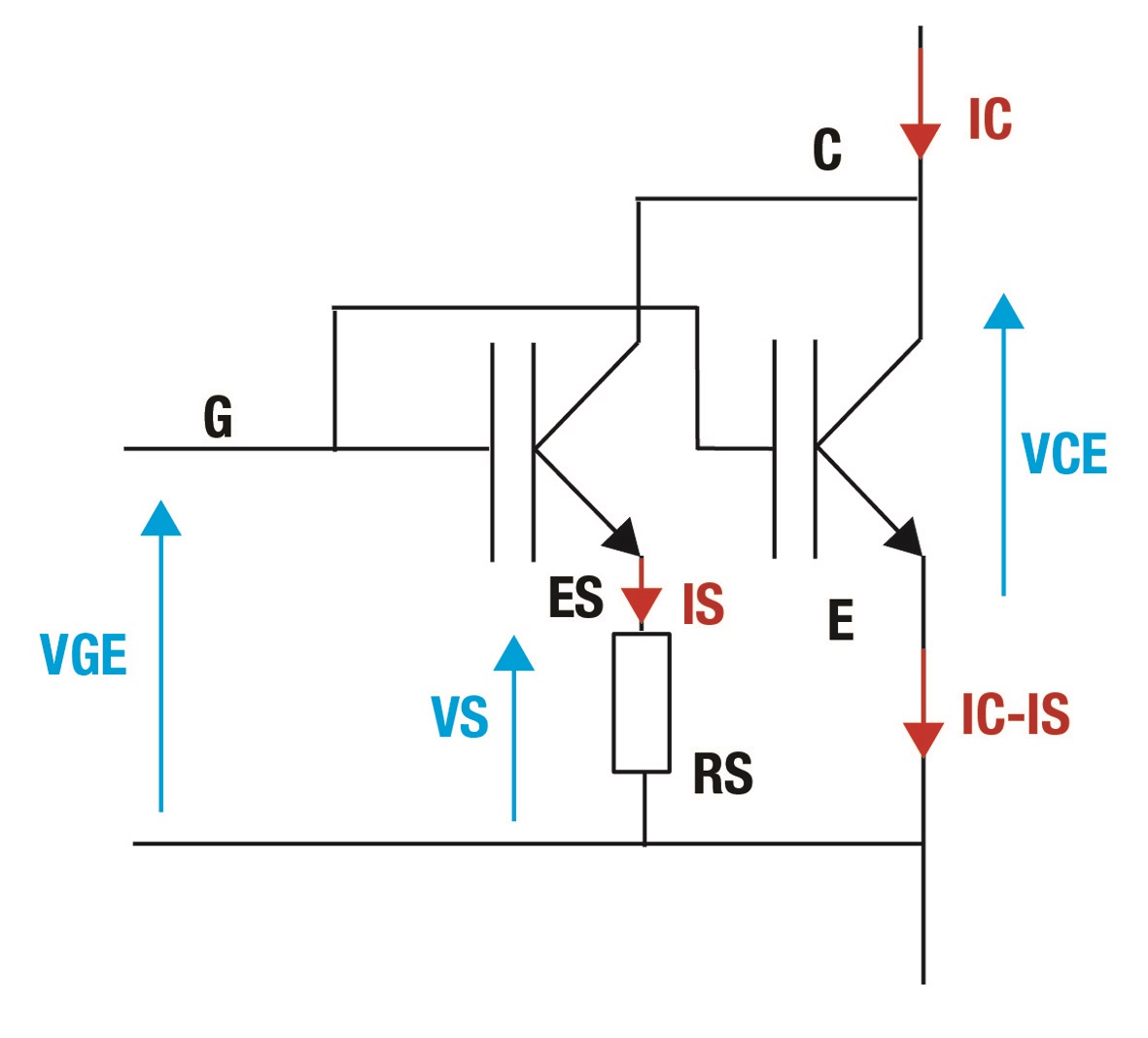
Figure 1: The basic concept of the current sense function
Bare die PCGA160T65NF8, PCGA200T65NF8, and PCGA300T65DF8 IGBTs can be available with or without integrated monolithic temperature and current sensing circuitry, in three current ratings. Their breakdown voltage of 650V is guaranteed over a junction temperature range from -40 to +175°C.
Bare die IGBTs are typically used by power module manufacturers to achieve a high level of power integration and reliability, or special power interconnections. The overarching objective is to push the power limits beyond standard module products.
Power device challenges
Power loss, thermal management, short-circuit, over-current or over-voltage and over-temperature protection, and current measurement are all design challenges for power semiconductors.
Power losses are affected by the VCEon value of an IGBT, and by its switching behaviour (turn-on and turn-off time) and switching frequency. These properties are impacted by the characteristics of the IGBT technology, the gate driving circuitry, the package stray inductance, and the thermal management system.
Since power losses can only be minimised but never fully eliminated, thermal management must aim to remove the heat created by the losses from the semiconductor. The best way to remove this heat is to improve the thermal conductivity between the silicon and the outside world. Advanced power modules adopt sintering techniques for the top and bottom of the power device, combined with double-sided cooling to improve thermal conductivity.
Over-voltage can be limited by controlling the amount of the stray inductance in the current path by the appropriate design and controlling the rate of change of the current.
Being able to detect and act upon over-current and over-temperature in time can extend the life of an inverter. Current measurement is required by the motor control system to control the amount of current and torque delivered by the motor.
Temperature sensing
Monolithic integrated temperature sensing in bare die IGBTs is accomplished by measuring the forward voltage drop (VF) of a string of polysilicon diodes, which are fabricated monolithically on the same die as the IGBT. Because the VF value of a diode shows a linear dependence on Tj as in the equation: ![]()
The method of monolithic current sensing proves to be the best way to measure the IGBT's junction temperature.
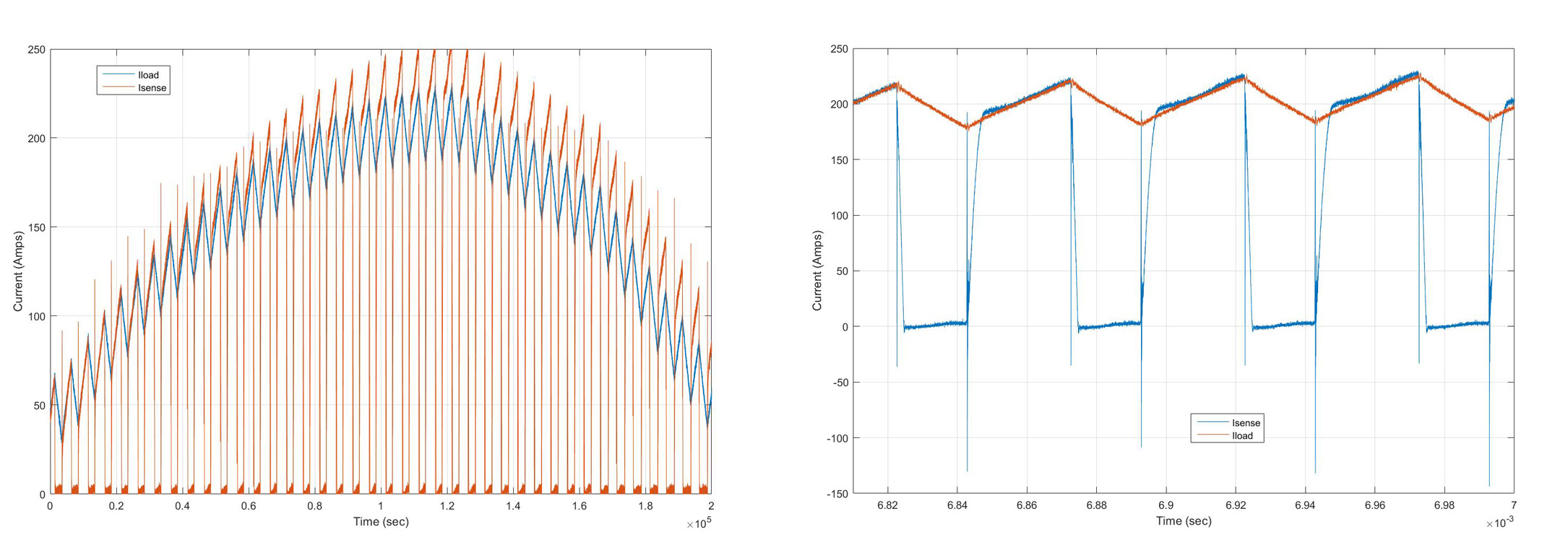
Figure 2: Some initial results achieved with on-die current sensing
The temperature sensor requires the diode to be forward-biased with precise constant current. The resulting voltage drop must be sensed and conditioned via an interface circuitry. Since the temperature diode is placed monolithically on silicon along with the power device, it is capacitive-coupled to the high voltage switching node of the IGBT.
The interface circuit must be designed to read the small temperature-dependent VF value, reject the switching voltages and pass the signal across an isolation barrier.
There are many ways of filtering the signal and passing it across the isolation barrier. An example is the use of an isolated amplifier and an ADC. This is combined with synchronous sampling to avoid the capturing of samples occurring with transient noise spikes.
Current sensing
Monolithic integrated current sensing is accomplished by measuring the current of a small IGBT in parallel with the main IGBT and then multiplying it by a known scaling factor. IGBTs consist of thousands of cells in parallel via a metallisation area on the top of the device. The small IGBT represents a portion of these cells that has been left disconnected from the rest of the cells and is made available as a current mirror.
The basic concept of the current sense function is shown in the equation: ![]()
A separate emitter connection provides a fraction of the main collector current (IS), which is connected to an external resistor (RS). This connection generates a voltage drop, which is proportional to the sense current. The sense resistor voltage is used to determine the current, and by knowing the main collector current (IC), a sense ratio (Ratio) is computed (Figure 1). The sense resistor (RS) can be replaced by an op-amp circuit that is designed to directly amplify the sense current in a current-follower configuration, eliminating the sense emitter voltage bias.
The current sense ratio is temperature-dependent, but, when combined with junction temperature sensing, it is expected that this interface will yield the necessary information to compensate for the junction temperature and produce a more accurate measure of the main collector current.
A bit more difficult is to correct the current dependency. This causes a limitation of the accuracy at low current, where low current are considered current levels below 10% of the full current range. The main limitation of monolithic current sensing is indeed the accuracy at a low current level.
Monolithic current sensing can be put to various uses in an HEV inverter. The most simple use is over-current protection, which may be accomplished easily with a comparator circuit to augment or replace the traditional desaturation protection.
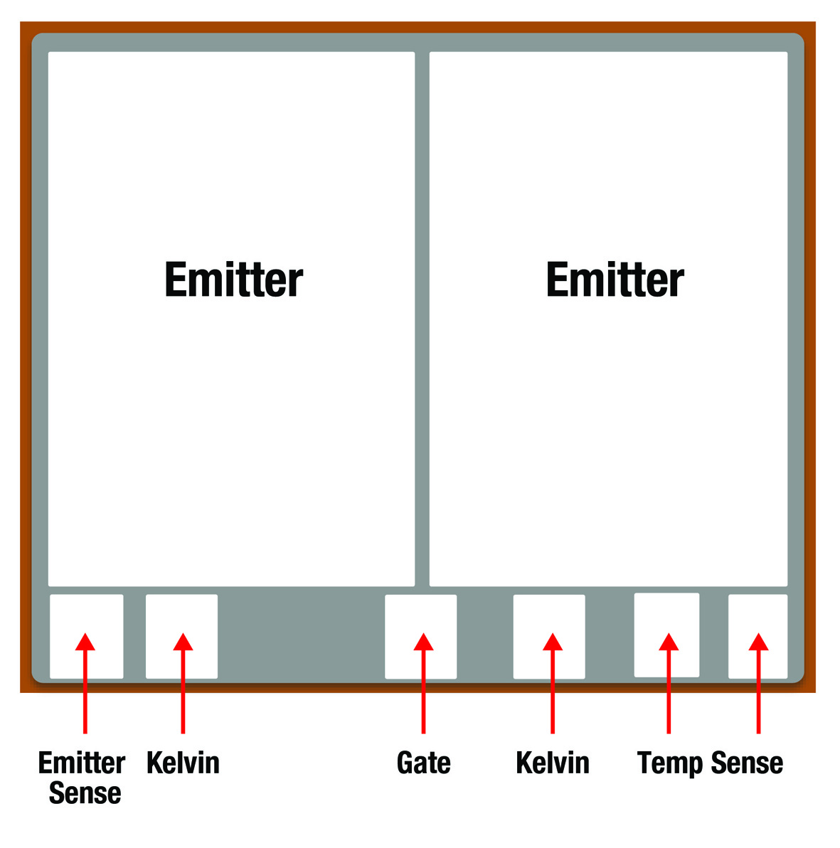
Figure 3: Layout of temperature and current sense pads on the top side of the IGBT
A much more challenging and potentially valuable use is motor control, which is feasible with additional interface circuitry and intelligent processing in combination with on-die temperature sensing. This application of the monolithic current sense function is in active development at Fairchild. Figure 2 shows some initial results achieved with the on-die current sensing.
Layout for sensing
An example of the bare die layout showing the temperature sense and current sense pads on the top side of the IGBT is given in Figure 3.
Monolithic integrated current sense and temperature sense circuitry provides a reliable way of measuring the junction temperature of an IGBT in power module applications, and of the collector current - without additional sensors. These techniques can provide substantial advantages for module manufacturers. It simplifies the sensing of key parameters, reduces component count, achieves a faster response to hazardous operating conditions, allows a more precise determination of junction temperature, leads to better use of the power silicon, and increases reliability. All of these characteristics will help inverter manufacturers or vehicle OEMs to achieve a more competitive position in the marketplace.
Product Spotlight
APV1111GVY
Panasonic

Panasonic PhotoMOS® Photovoltaic MOSFET High-Power Drivers
| SKU: | |
|---|---|
| Stock: | 3490 |
| Cost: | $3.95 |
