
Automotive design steps up EMI standards
Automotive and industrial design demands compact power supplies that meet low EMI standards, says Joey Yurgelon, Jesus Rosales, and Mark Marosek, Analog Devices
Automotive design steps up EMI standards
The dramatic increase of electronic content in today’s automobiles has multiplied the number of power supplies used, with many required to directly convert a wide ranging battery voltage to a usable regulated output.
Analog Devices has designed its LT836x family for automotive pre-boost applications, where battery input voltage can drop below the buck output voltage. The LT8361, LT8362, and LT8364 have a minimum input voltage of 2.8V to operate during cold crank or stop-start events. The maximum input voltage capability of up to 60V handles high input voltage transients, such as load dump.
Each converter provides the necessary boosting during low battery levels, and turn off with minimal power consumption during normal or load dump battery voltages.
A key requirement for any switching regulator is to provide enough power for a given application over the entire input voltage range while also guaranteeing reliability. The family provides voltage/peak current offerings of 60V/2 A (LT8362), 60V/4A (LT8364), and 100V/2A (LT8361) and high power switch voltage ratings extend output voltage capability and input voltage range for single-ended primary-inductor converter(SEPICs) and inverting converters.
Maximising power delivery
The power switches maintain their peak switch current limit over the entire duty cycle range. The advertised current of the switch is available without compromise, which is described as a significant advantage over converters that may exhibit a fall of 30% or more in peak switch current limit at high duty cycles.
Current-mode DC/DC converters typically add slope compensation to their peak switch current limit to avoid sub harmonic oscillations when that peak switch current limit is met, which means a reduction of peak switch current limit as duty cycle increases (as input voltage lowers). The LT836x family provides the full slope compensation necessary for proper operation at peak switch current limit, without the DC reduction of peak switch current limit versus duty cycle.
To meet the demand for compact power supplies, DC/DC converters use high switching frequencies to minimise component size and cost. The requirements for operation above the AM band in automotive applications has driven frequencies to 2MHz. Traditionally, high switching frequencies result in increased switching losses and limited duty-cycle range. The LT836x family minimises AC switching losses using fast power switch drivers and low minimum on- and off-times, to support a wide conversion range, even at 2MHz, says the company. The family can achieve lower losses and a higher duty-cycle range than many applications that would traditionally run at 400kHz to maximise efficiency. (Thermal performance is shown in Figure 1.)
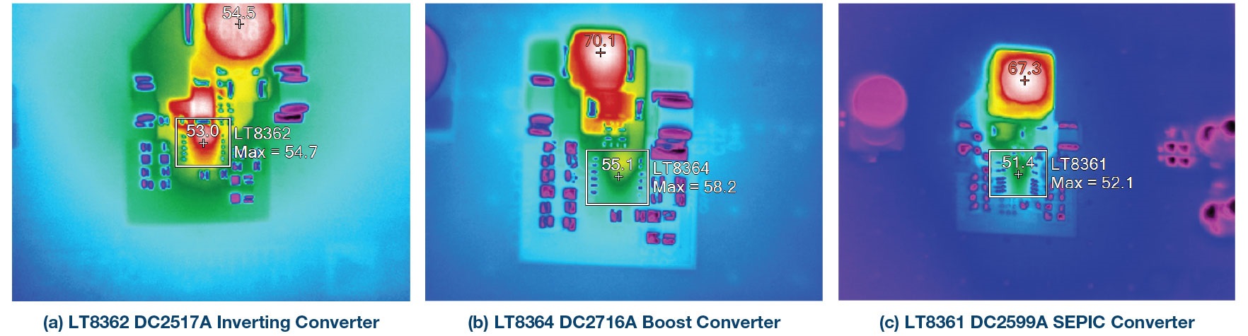
Figure 1: Thermal performance of LT8362 Cuk inverting, LT8364 boost, and LT8361 SEPIC
High efficiency at light loads
Optional Burst Mode operation uses single-switch pulses spaced evenly at a lower switching frequency to reduce switching losses, while minimising output voltage ripple. The converters can draw as little as 9µA from the input pin when in deep sleep or in pass through mode in a pre-boost application.
They are also capable of meeting CISPR 25 Class 5 standards using spread spectrum frequency modulation (SSFM) mode and proper board layout with some filtering.
Designers have traditionally avoided using switching regulators throughout EMI sensitive environments. A switcher’s large capacitors and troublesome hot loops elevate the importance of PCB layout to achieve good EMI performance and small size, placing a burden on board design and manufacture. The available factory demonstration circuits for the three converters include the requisite I/O filters and feature exemplary PCB layout to meet CISPR 25 Class 5 standards (as tested) when SSFM mode is selected. By essentially removing the converter from the EMI equation, application development time and cost are reduced (See Figure 2).
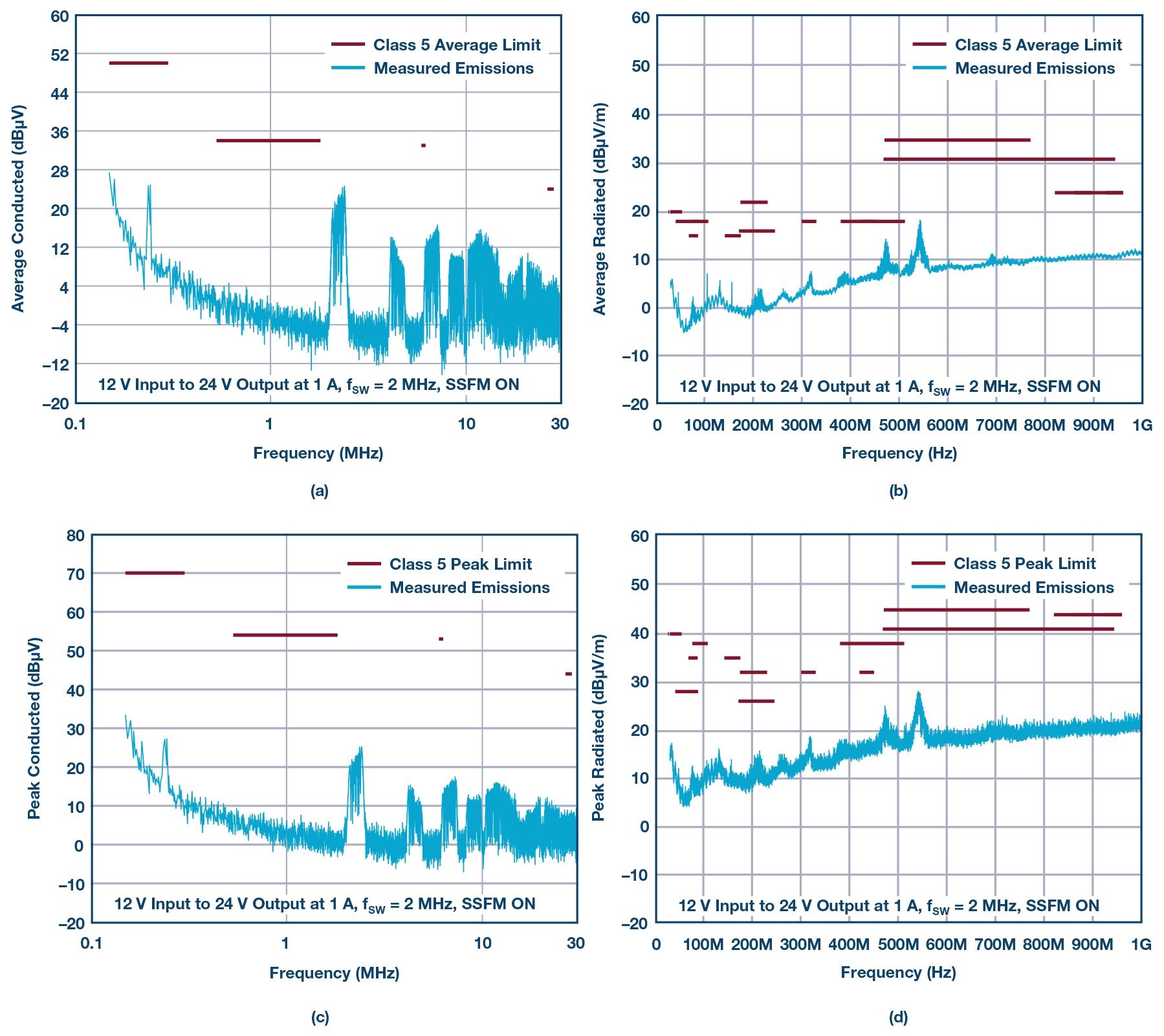 Figure 2: EMI test results for LT8364 boost
Until recently, selecting SSFM mode for low EMI meant having to use the less efficient pulse-skipping mode at light load. Adding a 100kΩ resistor from sync/mode pin to ground, however, allows the LT836x family to seamlessly transitions from SSFM mode to Burst Mode operation when loads become light. The result is low EMI and high efficiency over all loads (Figure 3).
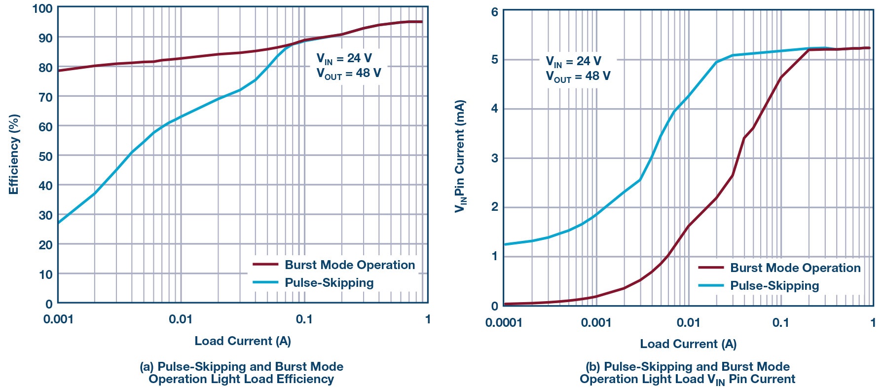 Figure 3: Pulse-skipping vs Burst Mode operation for LT8362 (24V input to 48V output)
By offering a single FBX pin that allows for both positive and negative output voltages, all topologies can be employed, to reduce design time and effort.
Boost converters
For large conversion ratio designs, operating in discontinuous conduction mode (DCM) might be the answer, while continuous conduction mode (CCM) can deliver higher output power.
Figure 4 shows an LT8364 low IQ, low EMI, 2MHz, 24V boost converter with SSFM that passes CISPR 25 Class 5 radiated and conducted EMI. It has an input of 12V to reach peak efficiency of 94%.
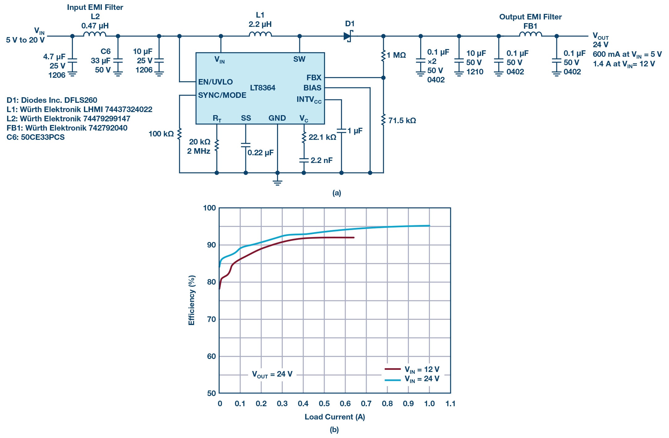
Figure 4: The LT8364 with peak efficiency of 94% and CISPR 25 Class 5 EMI
SEPIC converters
Automotive and industrial applications often operate from input voltages that can be above and below the required output voltage. For applications where the DC/DC converter is required to both step-up and step-down its input, a SEPIC topology is often used. SEPICs support applications that require output disconnect, ensuring no output voltage during shutdown and tolerating output short-circuit faults since there is no DC path from input to output. With switch ratings of 60/100V, and low minimum on- and off-times, wide input voltage ranges are achievable. The LT836x family offers an optional bias pin, which serves as a second input supply for the INTVCC regulator to improve efficiency.
The SEPIC converter in Figure 5 uses the LT8361 to showcase the versatility of a 100V rated switch. The switch voltage rating must be greater than the addition of maximum input and output voltages. With a 48V input to 24V output, the switch can easily handle the required 72V. Where the input is greater than the output, the bias pin can offer improved efficiency when connected to Vout. In this application, peak efficiency with a 12V input is 88%.
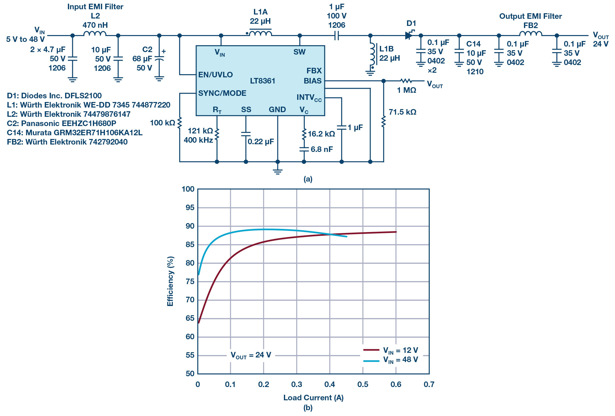
Figure 5: The LT8361, 400kHz, 24V output SEPIC converter passes CISPR 25 Class 5 EMI
Although negative supplies are commonly used today, many applications only have a positive input voltage from which to operate. The LT836x family, when configured in the inverting topology, can regulate from a positive input voltage that is above or below the magnitude of the negative output voltage. As with the SEPIC topology, the high 60/100V switch ratings and low minimum on- and off-times allow wide input voltage ranges.
Operating at 2MHz, the LT8362 offers an easy way to create a negative voltage from a positive input supply, as shown in Figure 6. The low IQ, low EMI, 2MHz, -12V inverting converter with SSFM and rugged 60V switch can operate with inputs up to 42V. With a Vin of 12V, a peak efficiency of 85% can be achieved. Operating with SSFM, this application passes CISPR 25 Class 5 radiated and conducted EMI.
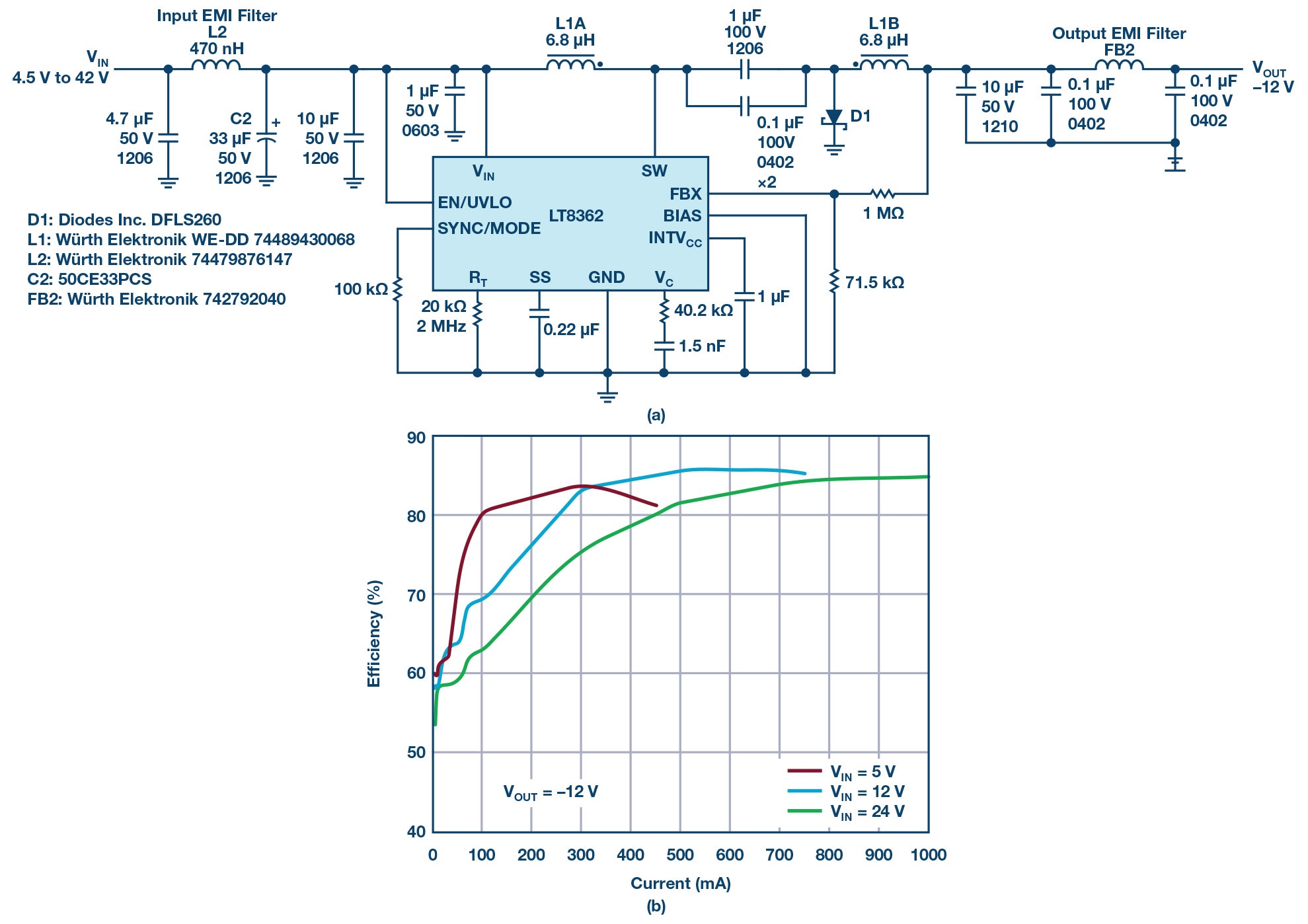 Figure 6: The LT8362 inverting converter passes CISPR 25 Class 5 EMI
According to Analog Devices, the LT836x switching regulators are a significant improvement over alternatives due to low IQ Burst Mode operation, flat switch current limit over duty cycle, low loss switching for 2MHz operation, and a wide input range. The switching regulators meet these demands in boost, SEPIC, or inverting topologies to deliver high power in small spaces while meeting stringent thermal and EMI requirements.
For customers who prefer leaded packages, each part is offered in a pin compatible 16(12)-lead MSE TSSOP with four pins removed for HV pin spacing. For smaller solutions, the LT8362 and LT8364 are also offered in DFN packages. All packages include a thermally enhanced exposed ground pad and are offered in E, I, and H temperature grades (Figure 7).
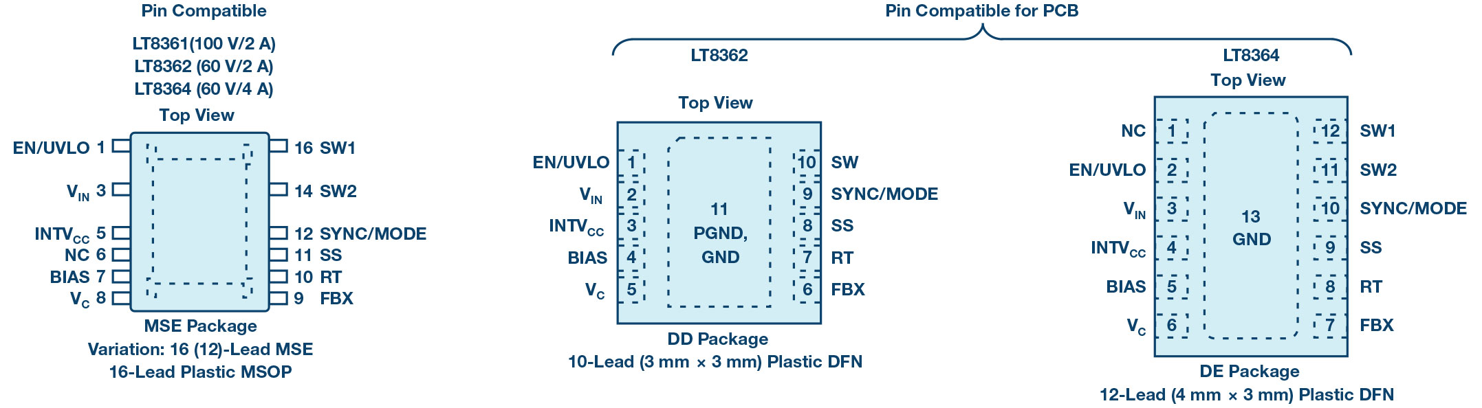
Figure 7: Pin compatibility of packages for the LT8361, LT8362, and LT8364
Product Spotlight
APV1111GVY
Panasonic

Panasonic PhotoMOS® Photovoltaic MOSFET High-Power Drivers
| SKU: | |
|---|---|
| Stock: | 3490 |
| Cost: | $3.95 |
