
What’s in your portable product?
Power-hungry handheld devices, medical products and industrial instruments require multi-cell or high capacity batteries to support ever-increasing processing needs, explains Tony Armstrong, Analog Devices
Batteries are virtually ubiquitous in a myriad of products and applications today. Commonplace examples include mobile phone and notebook computer; however, they are also commonly found in flashlights, cordless tools, MP3 players, portable video gaming devices, handheld multi-meters, as well as, scientific instruments and a plethora of healthcare devices.
The global market for portable battery-powered products was valued at an estimated $480billion in 2011 and is expected to reach more than $611billion in 2016. [Source: BCC Research]. The market is expected to continue its growth expansion through to 2020.
This market can be roughly segmented as communication products (29%), computer related products (29%), medical (19%) and cameras, toys, entertainment, timepieces, lighting, navigation and military products (23%).
This diversity has been accomplished because of a synergy between the product, the batteries they employ and the battery chargers and power-management systems that recharge the batteries.
Battery chemistry
What about the battery chemistry used inside them? The predominant battery chemistry is lithium-based, with demands fuelled by consumer device vendors, industrial goods manufacturers, the grid and renewable energy storage segment and automobile manufacturers. Within the industrial segment, healthcare, power tools and military applications represent the leading usage for lithium-ion (Li-Ion) batteries.
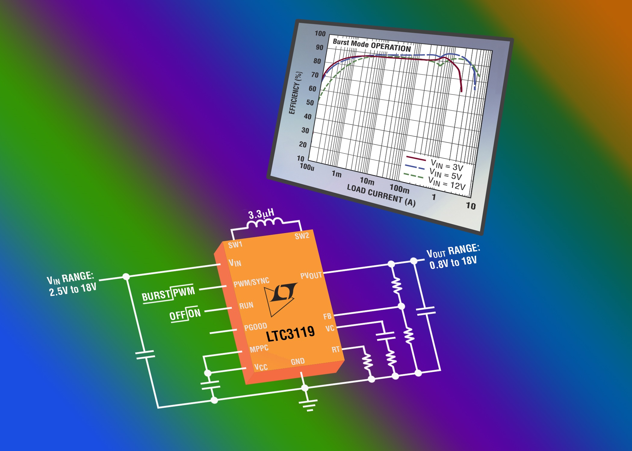
Figure 1: Schematic for LTC3119 showing integration and performance
A typical Li-Ion battery has a discharge profile from 4.2V when fully charged, down to 2.7V when fully discharged. While suitable for smartphones and MP3 players, it may not be suitable for portable scientific instruments, power tools and medical healthcare devices. In these instances, multiple cells may be required in order to supply the necessary run-time to be of practical use. This means that two to four cells will have to be utilised, either in series or in parallel, or a combination of both. As a result, the voltage range of these battery configurations could vary from 16.8 to 10.8V (four lithium cells in series), to 8.4 to5.4V (two lithium cells in series).
Layout considerations
High power density has become a primary requirement for DC/DC converters; likewise, power dissipation is a major concern for today’s feature rich, tightly packed devices, pushing the need for highly efficient solutions to minimise temperature rise. For applications where the input voltage source can be above or below the regulated output voltage, finding an efficient compact solution can be a challenge, especially at elevated power levels. Conventional design approaches, such as using a dual inductor SEPIC converter, produce relatively low efficiencies and a relatively large solution sizes.
Many loads require a regulated output that sits within the battery voltage range which necessitates the use of a converter that can both step-up and step-down. Although a SEPIC converter is a viable solution, its large size and modest conversion efficacy are sub-optimum for use in portable or luggable products. Thus, a wide voltage range, high efficiency buck-boost DC/DC converter is the solution for longer battery run times and handling multiple input sources.
A common problem of switching power supplies is ‘unstable’ switching waveforms. Sometimes, waveform jitter is so pronounced that audible noise can be heard from the magnetic components. If the problem is related to the PCB layout, identifying the cause can be difficult. As a result, proper PCB layout at the early stage of a switching supply design is critical.
Working with the PCB layout designer on the critical supply layout from the beginning can optimise supply efficiency, alleviate thermal stress, and minimise the noise and interactions among traces and components. To achieve these, it is important for the designer to understand the current conduction paths and signal flows in the switching power supply.
In a design without external heatsinks for surface mounted power MOSFETs and inductors, it is necessary to have sufficient copper area as a heatsink. For a DC voltage node, such as I/O voltage and power ground, it is desirable to make the copper area as large as possible. Multiple vias further reduce thermal stress. For the high dv/dt switch nodes, the proper size of the switch node copper area is a design trade-off between minimising the dv/dt related noises and providing good heatsinking capability for the MOSFETs.
Finally, the control circuitry should be located away from the noisy switching copper areas. It is preferable to have the control circuitry located close to the Vout+ side for a buck converter and close to the Vin+ side for a boost converter, where the power traces carry continuous current. If space allows, the control IC should be populated a small distance (0.5 to one inch/12 to 25mm) from the power MOSFETs and inductors, which are noisy and hot. However, if the space constraint forces the controller to be located close to power MOSFETs and inductors, special care must be taken to isolate the control circuitry from power components with ground planes.
Power converters
A power supply designer has to mitigate the risk involved with optimising a cumbersome solution like a SEPIC converter to generate a fixed output voltage when the input can be above, below, or even equal to the input. Optimising and integrating the power MOSFETs to facilitate a compact, efficient design simplifies the task. The LTC3119 is one option recently available from Analog Devices (see Figure 1). It is a synchronous current mode monolithic buck-boost converter that delivers up to 5A of continuous output current in buck mode from a variety of input sources, including single- or multiple-cell batteries, unregulated wall adapters as well as solar panels and supercapacitors. Higher output currents can be supported for pulsed load applications. The device’s 2.5 to 18V input voltage range extends down to 250mV once started. The output voltage is regulated with inputs above, below or equal to the output and is programmable from 0.8 to 18V. User-selectable Burst Mode operation lowers quiescent current to only 31μA, improving light load efficiency while extending battery runtime. The proprietary four-switch PWM buck-boost topology provides low noise, jitter-free switching through all operating modes, for RF and precision analogue applications that are sensitive to power supply noise. The device also includes programmable maximum power point control (MPPC) capability, ensuring maximum power delivery from power sources with higher output impedance including photovoltaic cells.
Up to four internal low RDSON N-channel MOSFETs deliver efficiencies of up to 95 per cent. Burst Mode operation can be disabled, offering low noise continuous switching. External frequency programming or synchronisation using an internal PLL enables operation over a wide switching frequency range of 400kHz to 2MHz, which allows for the trade-off between conversion efficiency and product size. The device can be used for RF power supplies, high current pulsed load applications, system back-up power supplies and even lead acid battery to 12V conversion systems.
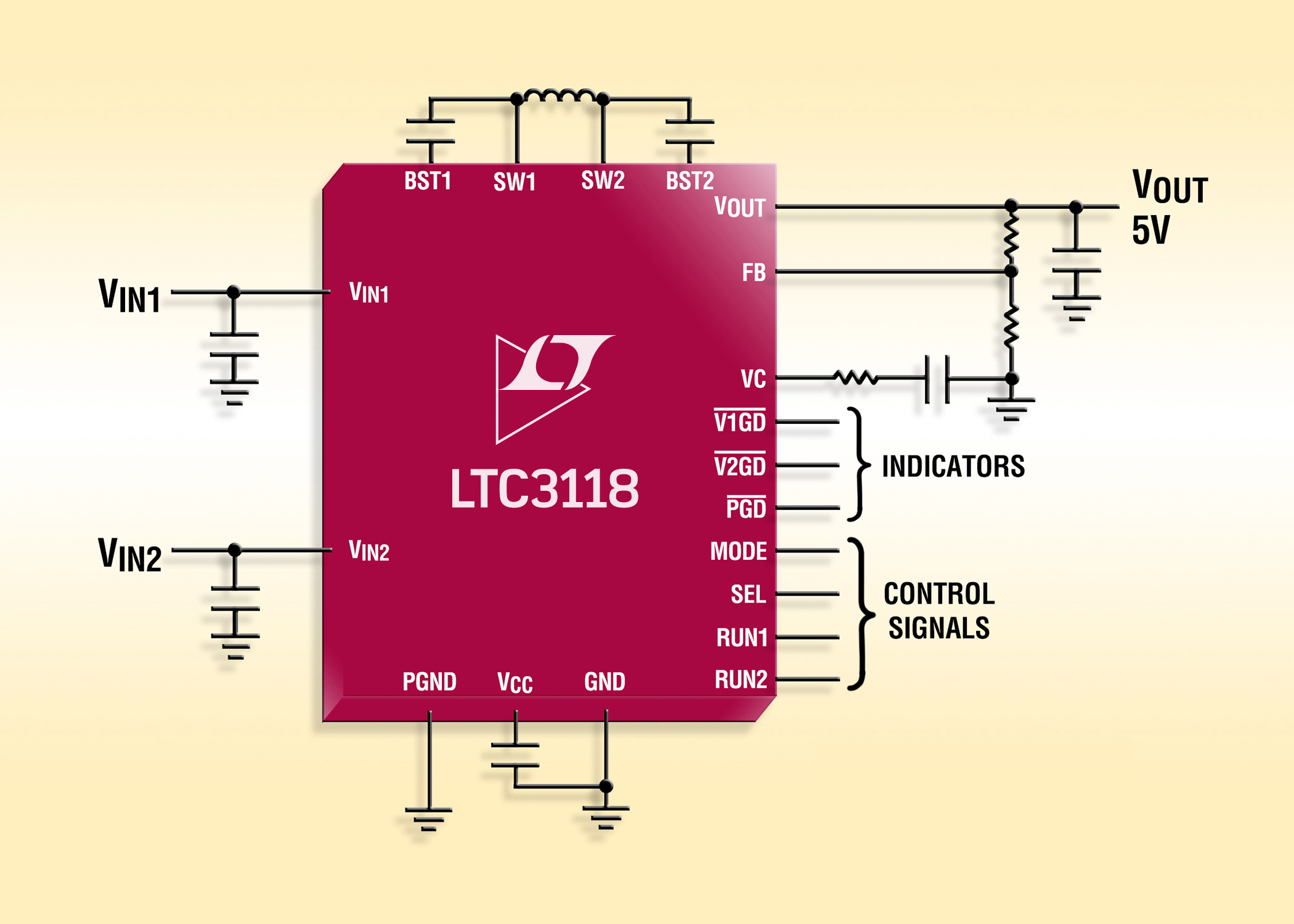 Figure 2: Schematic for LTC3118 with PowerPath section between two inputs
Many portable systems require being powered from multiple input sources including single or multi-call battery configurations, wall adapters and supercapacitor stacks. Another device in the same family is the LTC3118, a dual input, monolithic buck-boost with integrated lossless PowerPath which is capable of delivering up to 2A of continuous output current. It integrates the intelligence to automatically transition to the proper input source to seamlessly maintain a regulated output. Each input can operate from 2.2 to 18V, while the output can be programmed between 2.0 and 18V. A low noise, current mode buck-boost topology architecture has a fixed1.2MHz switching frequency for continuous, jitter-free transition between buck and boost modes, making it suitable for RF and other noise-sensitive applications. It has small externals and a 4.0 x 5.0mm QFN or TSSOP-28E package.
The LTC3118 (Figure 2) includes four internal low RDS(ON) N-channel MOSFETs to deliver efficiencies of up to 94% from either input. User-selectable Burst Mode operation lowers input quiescent current to only 50μA. For noise-sensitive applications, Burst Mode operation can be disabled resulting in fixed frequency, low-noise operation independent of load current.
Key design objectives
Designing a range of battery-powered portable products for communications, medical and computer related products presents some challenges in selecting the right power conversion, including spanning the input-to-output voltage constraints, power levels and ease of design, without compromising efficiency, run time and solution size.
Meeting system goals without a performance impact can be a daunting task. Buck-boost converters can simplify the design and maximise runtimes between battery recharging cycles due to their high efficiency operation across a wide range of loads.
Product Spotlight
APV1111GVY
Panasonic

Panasonic PhotoMOS® Photovoltaic MOSFET High-Power Drivers
| SKU: | |
|---|---|
| Stock: | 3490 |
| Cost: | $3.95 |
