
University launches Institute for Compound Semiconductors
In order to take research findings out of the lab and put them into the hands of those who can best exploit them, Cardiff University has launched the Institute for Compound Semiconductors (ICS). The aim is to bridge the exploitation gap, or 'valley of death'. The ICS aims to position South East Wales as the European leader in compound semiconductors, providing facilities that help researchers and industry work together to meet consumer demand by progressing academic research to a point where it can be introduced reliably and quickly into the production environment.
Semiconductors have been based largely on Silicon (Si) chips. Compound semiconductors (CS) take elements from groups III & V of the periodic table (either side of Si) e.g. gallium nitride (GaN). By varying both the quantity of the elements used and the way in which they are combined, the University can engineer properties of CS to suit its needs.
CS pervade our modern connected lives; they drive the internet, WiFi, smart phones, LED, photovoltaics and digital imaging, amongst others and, with the IoT gaining momentum, their role can only increase.
CS are the fastest growing sector of the semiconductor market. By setting up the ICS and thus providing a link between the research lab and the commercial world for one of the world’s key enabling technologies, the University is aiming for the city and surrounding areas to be recognised as the fifth cluster for semiconductors in Europe, but the first cluster for compound semiconductors.
This will be achieved through the growth of a cluster of companies who will wish to establish themselves in close proximity to the ICS, bringing jobs and investment to the area, which is already home to world-leading CS researchers, including Director of the ICS Professor Diana Huffaker, who joined Cardiff University from UCLA in 2015.
The region is also home to IQE, a global supplier of advanced wafer products and wafer services to the semiconductor industry. Microsemi, Infineon, Airbus, Stratium, Mesuro, Ivision, QMC, Global Laser and Q Chip are also amongst the companies with bases nearby.
The ICS stands in good stead to be part of a burdgeoning critical mass for CS expertise and innovation. In November 2015, Cardiff University and IQE announced a joint venture: the Compound Semiconductor Centre (CSC), which describes itself as Europe's new home for product, services and skills development in compound semiconductor technologies.
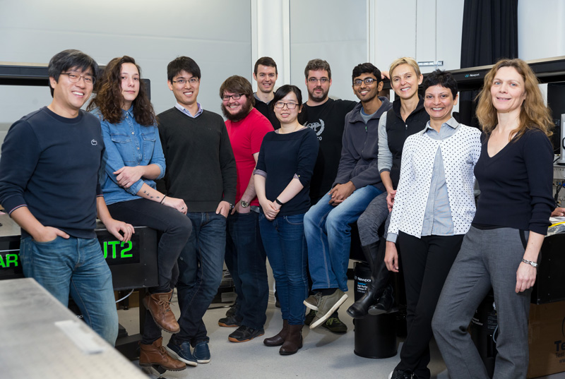
The ICS research team
Just a couple of months later, the UK Government announced that south Wales would be the home to a CS 'Catapult Centre', part of Innovate UK’s network of Catapults designed to transform the UK’s capability for innovation in specific areas of strategic importance and help drive future economic growth.
The UK government’s Engineering and Physical Sciences Research Council (EPSRC) has since invested £12m to set up at the University the EPSRC Manufacturing Hub in Compound Semiconductors, which will characterise and develop novel combinations of CS to develop technology that enables emerging trends, such as self-drive vehicles and 5G communications. In Spring 2017, the Cardiff Capital Region (CCR) Regional Cabinet agreed to invest £37.9m from the Cardiff City Deal Wider Investment Fund to support the development the cluster.
Most recently it was announced that £37.9m would be invested from the Cardiff Capital Region (CCR) City Deal to further support the development of a Compound Semiconductor industry cluster in south-east Wales. A facility will be constructed in the CCR to house Compound Semiconductor applications development and high volume Compound Semiconductor manufacturing, greatly helping the establishment of the world’s first Compound Semiconductor Cluster in the region.
Whilst research is already up and running at the Institute, the centre is about to embark on its defining project: the building and setting up of a research and testing facility. A bespoke cleanroom facility with small-scale, 4 and 8” (industrial scale) equipment and associated tooling, operated by highly skilled staff with experience in CS industries. The facility will allow ICS researchers to test the varying combinations of group III and V elements so as to tailor compound semiconductors according to their end use, be it in smartphones, automated vehicles or the vast array of technologies driving the digitisation of industry, healthcare and our homes.
Research at the institute already underway includes:
- Epitaxial layer optimisation
Establishing a systematic approach for epitaxial layer optimisation for gallium nitride (GaN) high frequency (HF) electronic devices. - III-V nanopillar optical links
Combining the advantages of III-V nanopillars with silicon photonics platforms. - InAs nanowire sensors
Reinventing an Indium Arsenide (InAs) nanowire avalanche photodiode (APD) on silicon substrate. - InAs/GaSb infrared detectors
Demonstrating high-performance photodetectors using an InAs/GaSb superlattice. - InGaAs single photon sensing
Demonstrating a new platform for state-of-the-art performances in single photon sensing at near infrared (NIR) range.
The Institute has received support and investment from EU European Regional Development Funds, the UK Research partnership investment fund (UKRPIF) and IQE. It has been established as part of Cardiff University’s £300m capital development plan.
Product Spotlight
APV1111GVY
Panasonic

Panasonic PhotoMOS® Photovoltaic MOSFET High-Power Drivers
| SKU: | |
|---|---|
| Stock: | 3490 |
| Cost: | $3.95 |
