
In-memory data deduplication technology doubles write speeds
The development of a high-speed in-memory data deduplication technology for all-flash arrays has been announced by Fujitsu Laboratories. These are large-scale, high-speed storage systems and use multiple flash devices such as solid-state drives.
This technology enables the production of storage systems with up to twice the response speed when writing data, compared to previous methods.
In recent years, all-flash arrays have incorporated deduplication technology that consolidates duplicate data into one to write to a flash device, in order to utilise the limited capacity of flash devices. However, as the system connects to multiple flash devices through a network in order to search for duplicate data each time it writes data, and storage devices grow in capacity and increase in speed, a problem of lowered response speed during write operations arises.
Now Fujitsu Laboratories has developed a new method that can accelerate response speeds by executing deduplication after writing data. In addition, as data may be written to memory twice in some cases when processing is continued with the new method, thereby increasing communications volume and lowering overall processing performance, Fujitsu Laboratories has developed technology to automatically switch between the new method and the previous method, as operational conditions require.
This means that response speeds can be increased by up to two times, improving the response of virtual desktop services and reducing database processing times.
Details of this technology were announced at the 28th Computer Systems Symposium (ComSys2016), held on 28th November at Hosei University in Tokyo.
Development background
In recent years, with the advance of virtualisation and the use of big data in business, performance requirements for storage systems have been increasing. All-flash arrays, which can increase performance by using high-speed flash devices and connecting multiple devices with a high-speed network, have therefore become widely used.
Flash devices are more expensive than traditional hard drives, and can only be written to a limited number of times over their lifetime, so all-flash arrays incorporate deduplication functionality that consolidates data to write only once to the flash device, which can increase the actual volume and reduce the number of unnecessary write operations (Figure 1).
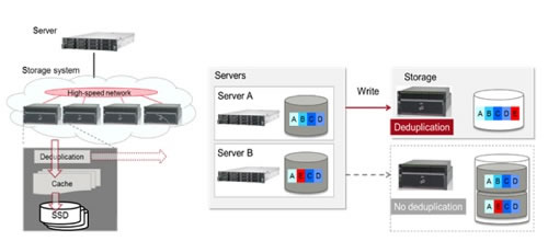
Figure 1: All-Flash Array Storage System and Deduplication
Issues
In order to utilise expensive flash devices effectively, in-memory deduplication technology was developed for all-flash arrays featuring deduplication functionality. However, because previous technology would institute a process to search for duplicate data before writing through a network that connects multiple flash devices, with storage systems that grow in capacity and increase in speed it created issues with longer response times when writing data due to the overhead required for search processing.
About the technology
Fujitsu Laboratories has developed a technology that can improve response speed for in-memory deduplication up to two times (Figure 2).
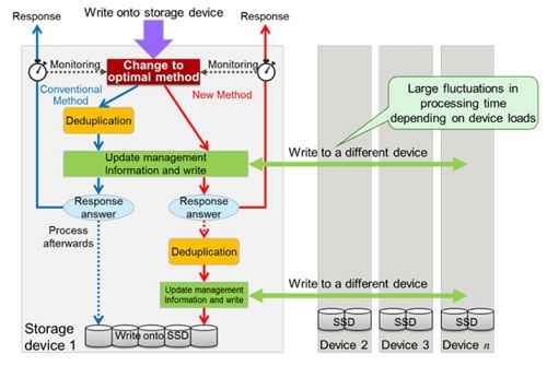
Figure 2: New In-Memory Deduplication Technology
Details of the technology are as follows.
1. New deduplication technology that improves response speed under low load
With the newly developed deduplication technology, the storage devices that make up the all-flash array cooperate to complete a write operation by temporarily storing the write data in open memory (the cache), improving response times. Then, while the server is preparing for the next write operation depending on the response from the memory, the technology searches for duplicate data, communicating between the storage devices in parallel, and the data is finally written to the solid-state drive after duplicates are eliminated. With this technology, response times for write operations can improve by up to two times when the storage system's network load is low.
2. Response time optimisation technology actively switches between two deduplication methods
Deduplicating after responding improves response speed compared to previous methods when the storage system's network load is low, but when the load is high the network becomes congested. This reduces response times more than previous methods due to data writes across multiple devices taking longer (Figure 3).
With the newly developed response time optimisation technology, of the two deduplication methods, the original method that writes after deduplication, for which the response time does not greatly vary, and the newly developed method, for which response times vary widely, the system automatically chooses the method with the shortest response time by calculating the expected value for the average response time, based on records measuring the actual response time.
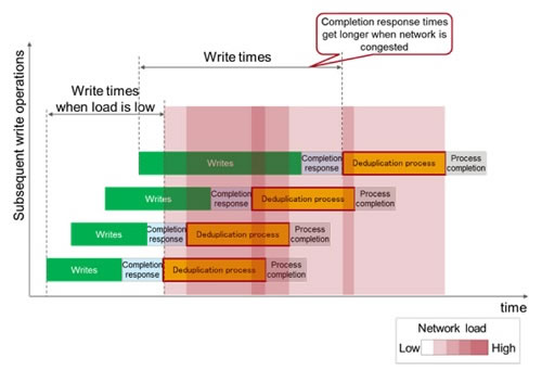
Figure 3: Network load leading to drop in write response speed
With this technology, by automatically choosing the optimal method in response to the continually changing status of the system, it is possible to reduce system response time as a whole (Figure 4).
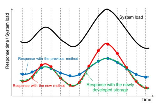
Figure 4: Response performance improvement with the newly developed method
Effects
Using the newly developed technology, Fujitsu Laboratories was able to achieve a lowest latency of about half that of previous technology in flexible I/O tester (fio) benchmarks. As a result, Fujitsu Laboratories was able to increase response speed when writing data to an all-flash array by up to two times. For example, in applications such as virtual desktops and data base processing that require high write speeds, as accessing small files occurs in enormous volumes, there are many duplications. In such situations, user applications on the service could be sped up, improving the user experience. In addition, by applying this system to back-end storage for operations databases, operations systems could be sped up, enabling further consolidation of IT infrastructure.
Future plans
Fujitsu Laboratories will continue development of technologies to further accelerate all-flash arrays going forward, aiming to incorporate them into Fujitsu Limited's storage products from fiscal 2017 or later.
Product Spotlight
APV1111GVY
Panasonic

Panasonic PhotoMOS® Photovoltaic MOSFET High-Power Drivers
| SKU: | |
|---|---|
| Stock: | 3490 |
| Cost: | $3.95 |
