
Controller importance in NAND Flash storage systems
Solid state drives (SSDs) based on NAND Flash memory are replacing hard disk drives (HDDs) in many applications, especially for portable and consumer devices. Steffen Allert of Hyperstone explains.
SSDs are also making inroads into enterprise storage because of their high performance and in industrial applications because of their robustness. The Flash controller plays a vital role in the system, providing the physical interface between the host and the Flash memory devices, and also making effective use of the Flash memory to provide the levels of reliability and performance required.
Figure 1 shows a simple block diagram of a typical Flash controller. There are three main parts to this: an interface to the NAND Flash memory, an interface to the host system, and the central processor that performs all the management functions. The ROM only provides initial bootstrap code - the firmware for the controller is stored in the Flash memory, making it easy to update. The choice of CPU is a key factor in determining the performance, features and power consumption of the controller.
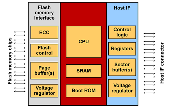
Above: Figure 1. Generic structure of a Flash memory controller
The host and Flash interfaces include buffers for data being read from and written to the Flash memory. This is required because of the differing speeds and data sizes used by the host and the Flash, and because the data from the host may need to be re-organised before being written. The controller should be able to transparently interleave accesses to multiple Flash memories, to achieve the required read and write speeds.
There are a number of characteristics of Flash memory that the controller has to manage in order to achieve the required performance, reliability and lifetime.
Address transaltion and mapping
The host will make writes to the Flash memory in chunks, typically based on the file system’s sector size and using ‘logical block addresses’. The controller has to manage the transfer of this data to the pages and blocks of the Flash memory, and keep track of the mapping between the host’s logical addresses and the physical addresses in the Flash, as shown in Figure 2. For speed, the mapping information will be kept in the RAM but needs to be saved to the Flash memory so that it is preserved when power is removed.
The type of mapping and update methods used will determine the performance and robustness, for example if power is lost unexpectedly.
ECC
As with all memory devices, there can be errors when data is read. These may be random errors induced by radiation, temporary failures caused by the stored value being disturbed when nearby cells are read or programmed, or failures to program cells. With Flash memory, these errors can become more frequent over time because of the limited program/erase cycles of Flash cells. The controller uses error-correcting codes (ECCs) to detect and correct errors. This means writing extra bits containing the ECCs when data is written to Flash. To check for errors, the ECCs are recalculated when the data is read and compared to the stored value. Typically, this allows single-bit errors to be corrected, and multi-bit errors to be detected. Repeated failures can indicate a bad block. The controller then needs to keep track of bad blocks so they are not used again.
A high-quality ECC implementation is, therefore, a vital part of ensuring data integrity in the Flash storage. There are many types of ECC that can be used. These are highly complex mathematical functions that provide different trade-offs in terms of correction speed and quality, hardware requirements and processing performance. The choice needs to be matched to the characteristics of the
Flash memory, such as the raw bit error rate and the distribution of errors. A good controller needs take these factors into account and have sufficient processing power to implement the best ECC algorithm.
Wear levelling
In order to minimise the effects of the limited program/erase endurance of Flash cells, and maximise the lifetime of the Flash, the controller uses wear levelling to ensure that all blocks are used evenly. This means that the controller must select the least used page from a pool of unused blocks when writing data. Again, there are several methods that can be used with different trade-offs for effectiveness and processing performance.
A characteristic of Flash memory is that data can only be written to erased pages. As a result, if random writes of data chunks smaller than a page are made, then the data currently in the page may need to be relocated to a new, erased, page. This is one of the main causes of write amplification – the fact that more writes are made to the Flash memory than are requested by the host.
The controller must ensure data integrity during this relocation of data and update the logical address mapping.
Because data is written in pages but can only be erased in blocks consisting of multiple pages, the controller will have to do garbage collection. This means copying data to consolidate used pages into blocks in order to release empty blocks that can then be erased for re-use. The timing and frequency of garbage collection needs to be managed to minimise the effect on performance seen by the host system. It also needs to ensure data is not lost in case of power failure.
The controller can exploit the over-provisioning of blocks in the Flash memory so that bad blocks do not reduce the usable capacity or lifetime of the Flash memory. The availability of spare blocks can also improve the performance of garbage collection and random writes.
Semiconductor reliability
An important factor for system reliability is the quality of the controller itself. This can be assured, firstly by rigorous design and test processes to ensure the device will work reliably in the specified environment. Also, because semiconductors are sensitive to radiation, the choice of packaging is important to minimise sources of alpha particles. Similarly, the packaging and interconnect materials need to be resistant to the stresses caused by changes in temperature during use. Production testing uses accelerated ageing to confirm that the devices will meet the requirements for failure rates and mean time between failures (MTBF).
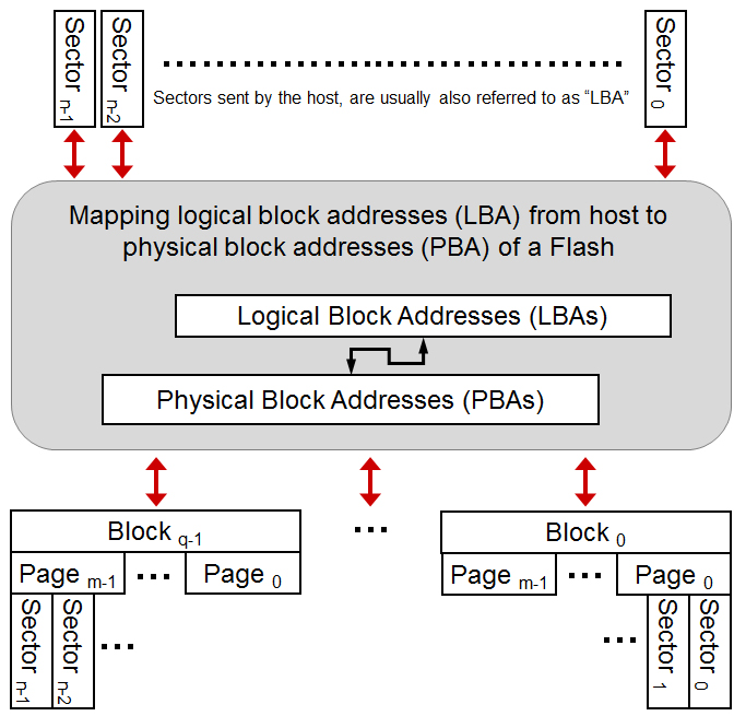
Above: Figure 2. Basic block-based address mapping
Health monitoring
Like any storage system Flash memory does have a limited life. The controller can monitor and record data such as the total number of erase and program cycles, the number of bad and spare blocks, and the error rates detected by the ECC.
This can be used to provide information to the host system and the user about the health status of the Flash memory. This enables early warning of potential failures so devices can be replaced before there is any risk of data loss. For SSD devices connected via the standard ATA interface, this information can be reported through the self-monitoring, analysis and reporting technology (SMART) protocol.
Conclusion
The controller is the key component for achieving reliable Flash-based storage by managing data transfers and ‘hiding’ the inherent shortcomings of the underlying storage technology. A high quality controller is essential to achieve the performance, reliability and lifetime required for data storage in consumer-level and enterprise but especially in industrial or embedded systems.
Product Spotlight
APV1111GVY
Panasonic

Panasonic PhotoMOS® Photovoltaic MOSFET High-Power Drivers
| SKU: | |
|---|---|
| Stock: | 3490 |
| Cost: | $3.95 |
