
The balance of power
Implementing innovative memory solutions may help add stability to the power/performance balancing act developers must not endure when selecting a new MCU. Philip Ling, ES Design magazine Editor, explores the issues further in this article.
It’s easy to overlook innovations in memory technology when considering microcontrollers; typically the ‘star of the show’ isn’t the memory structure but rather the processor core it supports. However, sometimes there’s enough glory to share around and in the case of Microchip’s latest announcement, that may be the case.
The core at the heart of the latest clutch of PIC32 devices is still a MIPS core, but it offers several new features; 16bit instructions, DSP extensions and a higher clock frequency, not to mention an MMU and I & D caches — all of which push the raw performance up to 330 DMIPS. This represents around a 3-fold increase over the existing PIC32MX devices. Furthermore, the PIC32MZ EC will be targeting embedded connectivity (hence the EC suffix), so it features a wide range of I/O interfaces — including (for the first time on a PIC device) a High Speed USB MAC/PHY combination.
While the core isn’t without its interesting features, such as the 159 DSP instructions that can enable algorithms to execute in as much as 75% fewer clock cycles, or the 16bit instructions that, Microchip insists, renders 30% higher code density over its competition. And a higher maximum clock frequency of 200MHz further helps improve overall performance (albeit for applications that aren’t typically focused on low-power), these are benefits that come with adopting the MIPS core. Where Microchip has arguably shown real initiative is in integrating a couple of memory-oriented features that could set a trend.
Dual-Panel Flash
Admittedly, the first isn’t exactly unique, but the use of dual-panel Flash builds on the need for read-while-write or, more importantly, dual-boot capability that many embedded devices now employ. The solution in the PIC32MZ actually offers something more; the ability to completely replace the program memory while the device is still running.
It achieves this through the use of (upto) 2Mbyte of Flash which can be arranged in two 1Mbyte panels, each with its own charge pump, and boot-flash memory and program-flash memory partitions (BFM and PFM respectively). It means the program memory can be completely reloaded without interrupting execution, passing control over to the new program once it has been verified. This offers a level of in-the-field software updating not commonly seen in embedded controllers. It offers both run-time self-programming (activated and managed in the application software) and in-circuit serial programming (performed using a serial data connection, and faster the run-time self-programming).
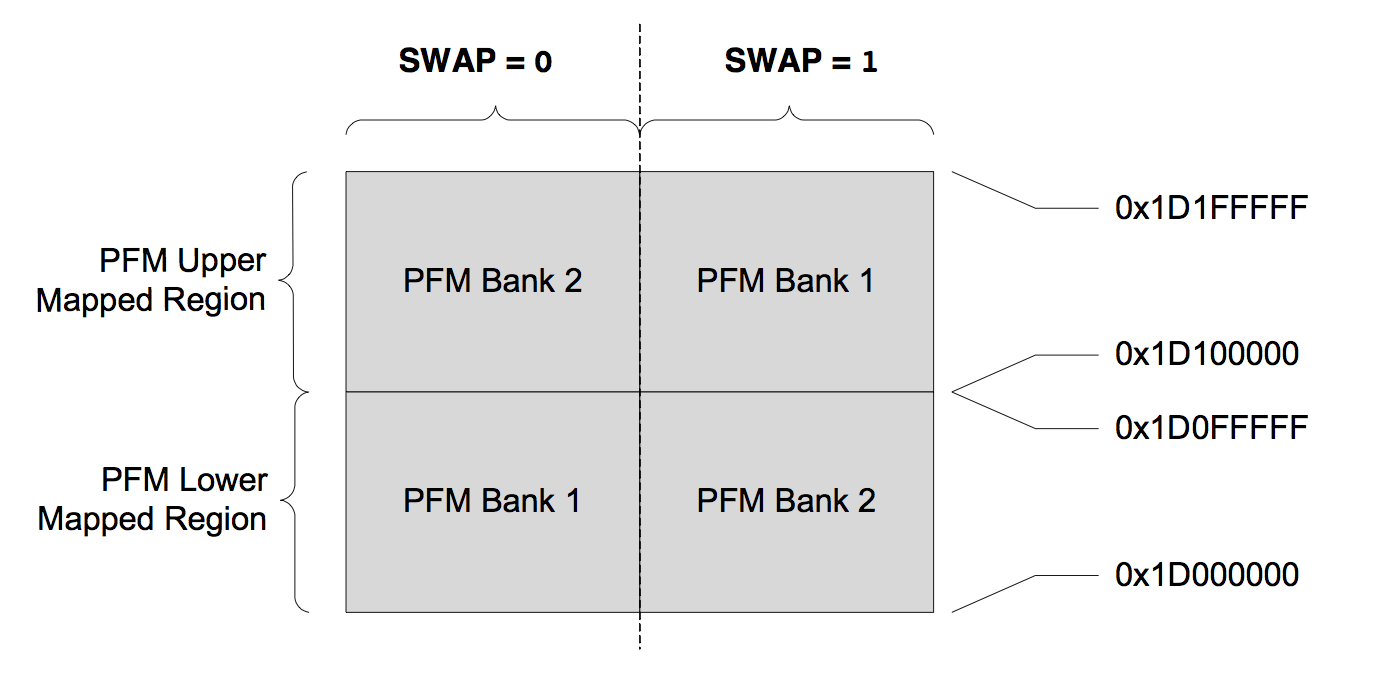
Figure 1: An example of Program Flash Memory mapping based on SWAP setting
Each bank of the flash memory has two logical partitions; the BFM and PFM. The two BFMs are aliased in to two regions at start-up; the ordering determines which BFM is selected at boot-time. The PFM regions of each bank are mapped in to upper and lower regions of the memory map; start-up code in the BFM can select the mapping of the two PFM partitions in to the two PFM regions. Each flash bank has an equally sized PFM region. The mapping of the banks of PFM in to address space is determined by the state of the SWAP control bit, as shown in Figure 1.
SQI
The need for innovative memory solutions is further enforced by the addition of an SQI interface; the first PIC device to feature the interface. The integrated SQI module is a synchronous serial interface that provides access to serial devices (typically memory) and supports Single Lane (which is identical to SPI), Dual Lane and Quad Lane interface modes.
It also supports two data transfer modes (DMA and programmed I/O modes), and Execute-In-Place (XIP). Support for SPI Mode 0 and Mode 3 is provided, with up to two chip selects and four bytes of flash address. Two 32-byte transmit and receive data buffers are included, as well as 4-word controller buffer (Figure 2).
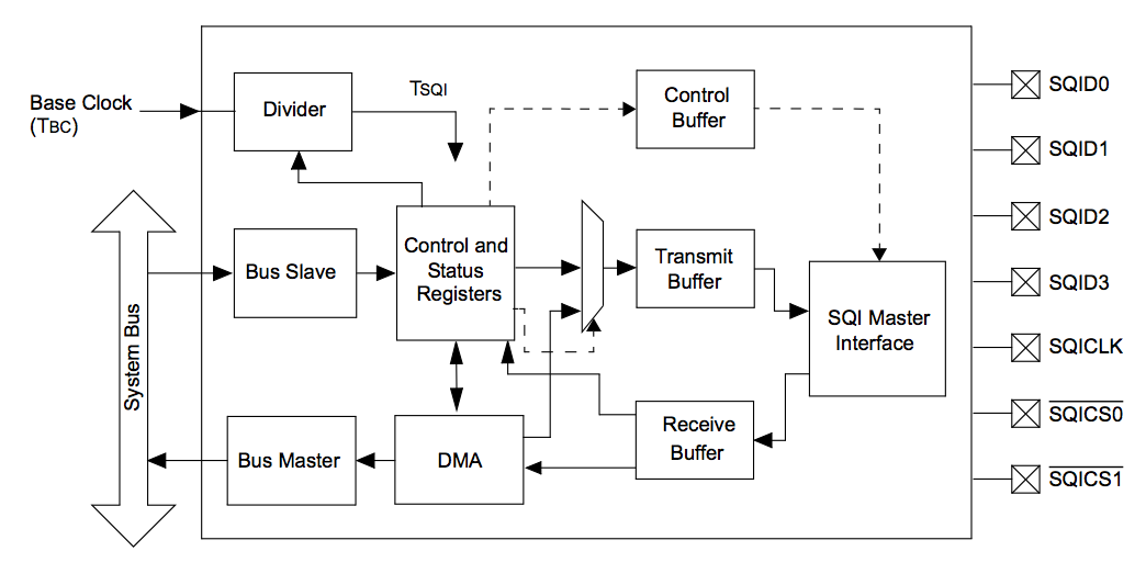
Figure 2: Block diagram of the SQI module
The DMA and programmed I/O modes are typically used to transfer data to and from external serial flash memory, whereas XIP mode can be used to execute the code out of an external serial flash memory.
In DMA mode, the SQI DMA engine off-loads the host processor by using predefined buffer descriptors for data transfer; each buffer descriptor can handle up to 64kbyte of data and multiple descriptors can be chained to support larger portions of data transfer.
Contrastingly, the programmed I/O mode is controlled by the host processor, configured a dedicated register. As it is slower than the DMA mode, and requires the host processor, it is expected to be used for smaller data transfers. The XIP mode provides adjustable timing and is, again, under the control of the host processor (using dedicated registers).
In conjunction with the microMIPS ISA, which is claimed to improve code density significantly by supporting 16bit instructions, Microchip is hoping the PIC32MZ EC will deliver the performance and rich peripherals needed by next-generation applications. Clearly it isn’t targeting the ultra-low-power end of the market as the newest examples of Cortex-M0+ enabled devices are, and perhaps that’s an important distinction. However, power will inevitably be an issue at some level for developers. By integrating greater choice in terms of memory options, along with the introduction of the DSP extensions, will help balance the power/performance trade-off all design teams must now go through.
Product Spotlight
APV1111GVY
Panasonic

Panasonic PhotoMOS® Photovoltaic MOSFET High-Power Drivers
| SKU: | |
|---|---|
| Stock: | 3490 |
| Cost: | $3.95 |
