
Be aware of datasheet thermal figures
Thermal management requires an understanding of how heat is transferred away from a semiconductor device’s junction. However, Siva Uppuluri, Applications Engineer, Diodes stresses that understanding how datasheet thermal figures are calculated and used is instrumental in assessing the thermal capability of a semiconductor device.
While the semiconductor industry has made great strides in pushing efficiency up and power consumption down in general, integrated circuits are still predominantly built on transistors - solid state switches. The fundamental nature of a switching device is that it passes a current and develops a voltage across it - the principle behind this demands a resistance to that current flow.
In turn, wherever current flows through a conductor with resistance there will be losses, the most predominant form of loss in an integrated circuit manifests itself as heat. Apart from representing wasted energy, heat at the junction of a semiconductor can, if left unchecked, cause rapid breakdown and failure of the device. Because of this, the method for the removal of unwanted heat in integrated devices can have major implications on performance and design. To design an effective heat sink, it is essential to understand and correctly interpret the thermal limitation data provided by the manufacturer.
Understanding the performance limitations of devices with respect to heat management is essential in product design, but it isn’t always as straightforward as including a fan or applying a heatsink.
Current flow and thermal resistance
Just as current flowing in a conductor is invariably met with resistance, so too is the flow of heat. Thermal resistance can also be calculated in a similar way to current flow - by taking into account the individual thermal resistances of the materials between the point of heat generation and its ultimate point of dispersion.
In general, heat can be dissipated in three ways - conduction, convection and radiation. By far the most significant of these, at least for a semiconductor, is conduction, as this describes the way heat travels through materials in contact with each other. In this respect, the heat generated at the transistor’s junction, for example, would be conducted through the substrate to the lead frame and then on to the heat sink connected to the lead frame.
Convective heat dissipation is defined as the transference of heat through a fluid - from a solid material through a gas or liquid, and from there to the surrounding atmosphere. In most systems, convection would represent the next most significant method of heat dissipation, after conduction.
Although radiation is a contributing factor, removing heat through radiation is largely disregarded in electronic systems as a viable primary solution because it relies on many variables, such as the proximity and mass of other solid objects, as well as ambient temperature.
For practical purposes, semiconductor manufacturers can assume heat dissipation is achieved primarily through conduction, and so provide the relevant information in datasheets. Typically this would take the form of a junction-to-ambient thermal resistance (Rth(JA)) and an absolute maximum junction temperature, Tj. From these figures it is possible to calculate the maximum power (Pmax) that the device can safely pass without causing self-damage.
This might appear to be relatively simple to calculate, given that the thermal resistance of the materials used from substrate to PCB should be known by the manufacturer. They may also provide alternative thermal resistance parameters, such as junction-to-case (Rth(JC)) or junction-to-lead (Rth(JL)). However, in practice it is slightly less straightforward than simply adding up the thermal resistance of the materials used.
Path of least resistance?
While an electrical current will follow a defined path, heat will find any way possible of leaving a material - for a semiconductor package that means there will be multiple paths. Each path has its own thermal resistance, the value of which will be defined by the size, shape and thermal conductivity of the path.
Consequently, the thermal resistance figure(s) given in a datasheet will only be applicable to a specific point on the package, and will also depend on the accuracy of the heat measurement taken. Even using highly accurate temperature measurement methods such as non-contact infrared, taking an accurate reading remains difficult and, to some degree, subjective.
In an effort to standardise the way thermal resistance measurements are recorded and reported, JEDEC introduced the JESD51-12 standard, which has two main goals - to standardise the way suppliers record electronic package thermal information, and to enable end users to properly understand, interpret and use that information. To this end, it defines two methods for determining Rth(JC) and Rth(JL) that ensure consistency across manufacturers.
The first method is used to determine the thermal resistance between two points of a heat flow path - one point being the junction and the second point being an arbitrary point on the package, such as the top, side or solder point. Importantly, this method assumes that a suitable heatsink is attached at the point of measurement, causing all of the power dissipated to flow to this point and thereby allowing other paths to be treated as insignificant (see Equation 1).
Equation 1: Rth(JX_Ө) = (Tj –Tx) / P
As the figure derived represents the main path, it conducts close to all of the heat flowing. As no other paths are taken into account, it is absolute, and isn’t influenced by the amount of power dissipated or other physical properties (such as the board on which the device is mounted). However, it is influenced by the packaging and so is useful for comparing the thermal performance of devices using different lead frames, for example. Diodes Incorporated uses this method to define Rth(JL) in its datasheets.
The second method defined by the standard provides a thermal characterisation parameter, as opposed to thermal resistance. This assumes no heatsink is attached at the point of measurement and, consequently, it is influenced by the total power dissipation. This figure is given by Equation 2, which results in a derated value for Rth(JC) and is more accurately referred to as Ψth(JC). Diodes Incorporated uses this method for calculating Rth(JC) in its datasheets.
Equation 2: Rth(JX_ᴪ) = (Tj –Tx) / P
Not ideal conditions
These datasheet figures are normally attained under certain defined conditions, which may not always reflect the operational conditions. In practice, devices are normally closely positioned on a board, while the lead frame tab of the device in question may or may not be in contact with a heat sinking material equal to that used to calculate the datasheet figures. This variability makes it difficult to use Rth(JL), Rth(JC) or Ψth(JC) to accurately calculate the junction temperature, Tj.
It’s a common misconception to treat Rth(JL) and Rth(JC) as values independent of heatsink and operating Tj. However, the graphs in Figures 1-3 show the different results that can be attained for each of the three thermal resistances discussed so far, based on two scenarios - using a 2”x 2” aluminium board (red) and the manufacturer’s recommended pad (MRP) layout (blue).
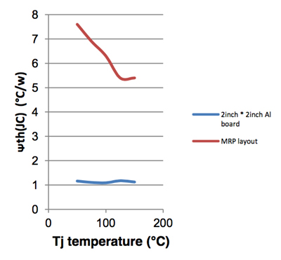 Figure 1. ᴪth(JC) vs. Tj
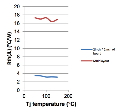
Figure 2. Rth(JL) vs. Tj
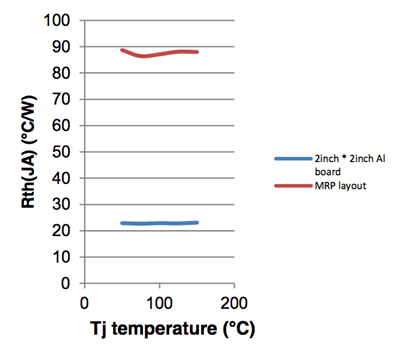
Figure 3. Rth(JA) vs. Tj
The graph relating to the resistance of the path from junction to lead (Rth(JL)), attained using JESD51-12 Method 1, clearly shows the impact of a heatsink which deviates from the ‘perfect’ heatsink. This is significant because in practice it would be impractical to employ a ‘perfect’ heatsink such as that used by the manufacture to calculate this figure. Consequently, this figure is best used to compare the thermal conductivity of the device’s lead frame, when evaluating similar devices in different packages, or from different manufacturers.
The graph depicting the temperature difference between the junction and point of measurement on the case (Ψth(JC)) is, as stated earlier, really only a thermal parameter (not thermal resistance) and, as such, is also best used to compare the differences in lead frames between devices using different packages and, where appropriate, from different manufacturers. It is appropriate to explain why this figure falls as the junction temperature increases. This is predominantly due to the effect of convection, caused by the air around the device heating up and then moving, something that would happen even in still air conditions. As the figure in question is small in comparison to the thermal resistance measurements, this reduction appears more significant that perhaps it is. Because of this phenomenon, it should not be used exclusively when calculating the junction temperature under operating conditions. However, conversely, because Ψth(JC) is generally small, any error in calculations will also be small.
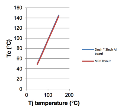 Figure 4. Tc vs. Tj
The final graph in Figure 4 charts the junction temperature in relation to the case temperature. This figure is much less dependent on the size and position of the heatsink and provided that the temperature on the case can be measured accurately, provides an effective way of calculating the actual junction temperature.
Conclusion
It is clear that, despite JEDEC’s efforts to standardise the methods used for calculating thermal resistance figures, they can still only be used as a guide. The figures published by manufacturers in their datasheets are still very dependent on the heatsink arrangement used in real world applications.
Measuring the temperature of the case accurately and plotting it on a graph that shows the relative junction temperature is an effective way of designing for thermal management. While the thermal resistances offered by manufacturers can be useful, it must be remembered that they are generally there for guidance and comparison purposes.
Product Spotlight
APV1111GVY
Panasonic

Panasonic PhotoMOS® Photovoltaic MOSFET High-Power Drivers
| SKU: | |
|---|---|
| Stock: | 3490 |
| Cost: | $3.95 |
