Metrology system analyses semiconductor packaging
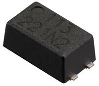
Advantest has a new mold thickness metrology system, the TS9000, for measuring the thickness of semiconductor packaging. The system is based on advances in Terahertz (THz) technology pioneered by Advantest. The TS9000 Mold Thickness Analysis (MTA) System is a new metrology tool that performs non-destructive analysis of the thickness of semiconductor packaging.
Meeting the high standards of speed and accuracy required for high-volume manufacturing, its innovative inspection capabilities are expected to contribute significantly to product quality improvement amid the trends towards smaller device sizes and higher integration, driven in part by the widespread adoption of smartphones and tablets.
Future systems from the THz product family will target the pharmaceutical, automotive, ceramic and other industrial markets in addition to semiconductors. .Advantest is leveraging its leading capabilities in terahertz technology to bring cutting-edge non-destructive analysis to industrial production lines.


