
Why are SiC and GaN so important?
The higher switching frequencies, operating temperatures, and voltage handling capabilities of Wide BandGap (WBG) materials such as Gallium Nitride (GaN) and Silicon Carbide (SiC) makes them of fundamental importance to any effort to reduce energy consumption.
In this Q&A, Steve Lambouses, Vice President and General Manager for high voltage power at Texas Instruments explains why they are so important, and what we need to do to deploy devices based on these materials more quickly.
The Energy Imperative 2017: Why are SiC and GaN so important?
Steve Lambouses: Both are WBG materials and significantly reduce conduction and switching losses relative to silicon counterparts, such as IGBTs or super junction MOSFET technologies.
They have higher switching frequencies so things (components, such as inductors) shrink down, so power density gets greater and energy losses decrease. And they really play into higher power applications.
So, when you look at data centres or anywhere where you have lots of processing going on, and which requires a lot of ac power, you can see how they would play a big role in conserving energy. This also includes power hungry applications like in EVs and ATVs (electric vehicles and all-terrain vehicles).
E.I.2017: How would you divide applications for SiC and GaN?
Steve: Both are WBG, but serve two different applications because of their different characteristics. GaN tends to be used for <1,000V, sub-3kW applications. This includes power supplies and data centres SiC gets above 1,000V and gets into much higher current levels, such as 50A and above, where you get into 5Kw, 10kW type of systems which lend themselves into transportation systems, like EVs, ATVs, trains and even into solar.
E.I.2017: How do they affect power supply design?
Steve: What’s unique about some of the characteristics of GaN (such as no reverse recovery) is that it allows you to get into new power technologies, like a totem-pole PFC (power factor correction) stage, which couldn’t be done with a typical silicon device. It’s really opening up whole new unexplored areas of power topologies that extract all the benefits of wide bandgap.
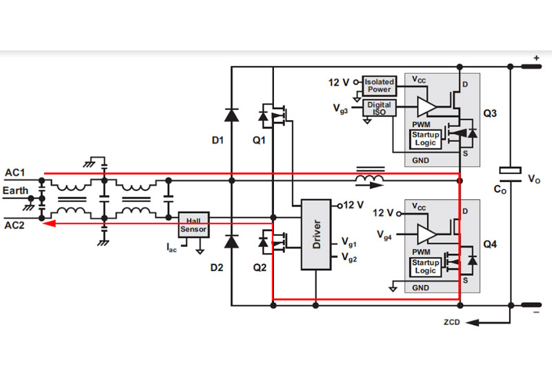
E.I.2017: Why are totem-pole PFCs so important and why are they now possible?
Steve: On the front stage of a power supply (AC input) you have PFC, then the DC/DC phase. You need to optimise efficiency of both stages. The fact that GaN doesn’t have reverse recovery (requirements, like Mosfets) allows you to get into a different architecture for PFC – called the totem-pole PFC – that gets you to 99% efficiency (Figure 2). That’s unheard of.
Figure 2: With GaN, new PFC architectures that were once inhibited by the reverse-recovery requirement of Mosfets are now possible and can realize efficiencies of up to 99%.
Then in the second stage, DC/DC there’ll be losses there, of course, and then you get to the point of load (POL). Still, using GaN there are efficiency gains to be had (vs Si).
So all the way from wall to load, we can improve PFC and DC/DC by three percent over what it is today. This may not sound like a lot, but when you’re going from 92% or 93%, which is best in class today, to over 96%, and you’re talking about datacentres that consume 70bn KW per year (in the US), a three percent savings is pretty huge.
Now, note that some Si devices can get to 94% but you’re using exotic components and layouts, trying to squeeze out a 10th of a percent savings in efficiency.
Also, by switching at the higher frequency, efficiency is so much better and the cooling system (air or liquid) can now be significantly reduced. Internally we say, 'Lose the fan with GaN'.
E.I.2017: What’s the WBG effect on automotive?
Steve: We’re talking to automotive manufacturers looking to eliminate liquid cooling from their power inverters and going to pure air cooling. This saves on cost, weight, and maintenance, while improving reliability. Big benefits.
In fact, the automotive industry has come out with fuel-efficiency savings numbers: 10% more miles per gallon using WBG SiC.
With higher efficiency and higher voltage (industry’s move to 48V batteries in automobiles) you have lower current requirements, so cabling gets smaller and that all goes to weight reduction. Japan, for example, is moving to SiC for trains and has substantial savings in weight on train, which translates to a lot of things like maintenance and cost to operate.
The benefit of GaN with the engine off is that you can power ancillary functions without draining the battery.
E.I.2017: So what’s needed to propagate these technologies?
Steve: While versions of GaN have been out there for quite some time, specifically in the RF and lighting space, the power side of GaN and the power switches, is very new, only the last few years. The major roadblocks to adoption we see are reliability and ecosystems.
Reliability: We don’t have the history we have with silicon in real-life applications. It is new territory for all of GaN power-switch manufacturers to really go and understand the differences between GaN power switches versus silicon and how we evaluate, test and qualify them.
At TI we have invested heavily in internal proprietary methods to really go and ensure that these devices are not only reliable but that we understand real-life applications and are mimicking them internally as we’re going to qualify our devices.
We are also working across the industry with other GaN suppliers and customers, consortiums, industry groups, and special interest groups to really come out with some standards around that so that our customers can feel comfortable that when they’re getting a switch from one manufacturer or another that it’s all under the same umbrella of reliability.
The Ecosystem: It’s great that we have this GaN switch that can switch at these really fast frequencies, but if you don’t have an equally paired and fast driver to exercise that switch to turn it on and off and protect it, then you won’t get the full benefit of the efficiency gains of GaN.
Also, in front of that driver, you need a power-conversion controller that can exercise that driver and take advantages of topologies like totem-pole PFC. Finally, if it’s not all co-packaged correctly, you still won’t get the full benefit of the system. This includes optimised designs and pc-board layout.
E.I.2017: What about SiC?
Steve: The SiC power switch has been out there a lot longer, and the infrastructure is built around it. There’s not a concern about reliability, as it’s pretty well known. What is missing is the infrastructure, like the optimised gate drivers and optimised controllers to take advantage of those higher switching frequencies.
We also need to be better about fault reporting. Things are happening faster so the system has to be able to adapt on the fly and be smarter, such as with an overtemperature or overcurrent event. You need to be able to shut things down orderly and quickly and report that out.
For example, SiC switching frequencies are in the hundreds of kHz, while IGBTs are in the 10s of kHz. GaN easily gets in to the MHz, but you need the right packaging, with the driver co-packaged with the switch. At TI, we believe in co-packaging as it optimizes the performance of the power switch.
E.I.2017: Do drivers need a new approach too?
Steve: They definitely need to be able to respond a lot faster. Also, because you’re paralleling these devices, you want to know that when one driver turns on, the other one is going to turn on within a fixed time that’s well understood and very well controlled, so your channel-to-channel matching on the drivers is going to be absolutely critical.
The other thing is that these drivers are operating at a much higher voltage, so you’ve got to be able to isolate primary and secondary sides. If you look at some of our recent drivers, they’re coming out with 600 or 700V and in some cases, like with SiC, we’re seeing the need for gate drivers with isolation up to 5,000V.
This involves silicon process, mold compound, packaging, lead frame, wire sweeps, all the stuff that has to come together. Also, when switching at these higher frequencies, inductance of packaging becomes a major factor.
As a result of the fine tuning that needs to be done, in the case of GaN, we are manufacturing the switch internal to TI and we are co-packaging it with our driver into what we call a power module. This includes a driver plus the switch, or a driver plus two switches and a half bridge co-package. We have no plans for a standalone switch at this point.
E.I.2017: How close are we to standards to be able to quantify WBG reliability?
Steve: We have an intrinsically qualified wafer process for GaN (for over a year now). We do know for a fact that – and our partners and other GaN switch manufacturers will say the same thing – that things like JEDEC specs really don’t apply to GaN as it’s a whole different beast versus pure silicon. Doing traditional burn-in and latch up and traditional tests, you can pass with GaN and fail with GaN, as it’s so different.
So, internally we’ve invested heavily in actual switching applications through the rigors of what they would see in an actual customer application that allows us to get a quite a large number of life-time hours of hard switching. We also built up an infrastructure of pure power stages where we can get lifetime data under normal life operation.
This has given us a database to mimic the 30+ years of silicon expertise customers have using pure FET. We are getting ready to present some of that to some working groups we are a part of at APEC 2017.
Across the industry we have been one of the pioneers in really pulling other GaN suppliers together with customers, and with spec groups, because we know that this will be key for customers to feel comfortable about using devices.
E.I.2017: Does this mean we’ll have some consistency across WBG device specifications?
Steve: I can’t say all devices will look the same, because one of the unique things about GaN is that the gate voltage can be different from one manufacturer to another: so they won’t necessarily be drop-in replacements.
But, the method by which we qualify, the documentation and specifications and datasheets, we all are aligned that those things should be pretty standard so that even if the gate voltage is slightly different, and it’s not a drop-in replacement, you can get a feel for the quality level of the device, no matter who you get it from.
E.I.2017: How would engineers compare and select WBG devices given the inconsistencies?
Steve: There are standards forming around qualification and documentation so designers will be able to compare key parameters such as conduction losses, switching frequencies, gate drive, and reliability requirements (as determined by the group) so the will be able to compare apples to apples.
But stepping back, they need to understand the entire ecosystem. That’s the value we bring in allowing designers to get into production faster. You can’t just take out a Si Mosfet or the IGBT, and drop in a GaN and SiC. You really have to redesign the whole system and you need people who understand that system to help you with that.
E.I.2017: Is there anything afoot to further help with power conservation?
Steve: Definitely! In the area of IC packaging to minimise inductance (as mentioned earlier) or with unique packaging that allows you push the boundaries of power that you can push through a package. For example, to get 1.5 or 2KW into an 8x8 or smaller QFN we produce. When you can push more power in, you can push different topologies and shrink systems quite a bit.
We also need to advance isolated process technology because as WBGs become more prolific there’ll be more applications so we’ll have different versions of isolated gate drivers, so that’ll continue.
Finally, we are just scratching the surface of GaN: as customers start to use them more and more we’re looking at different flavours and different variants.
Product Spotlight
APV1111GVY
Panasonic

Panasonic PhotoMOS® Photovoltaic MOSFET High-Power Drivers
| SKU: | |
|---|---|
| Stock: | 3490 |
| Cost: | $3.95 |
