
The case for on-board voltage monitoring IP
As Cadence’s Bob Salem explains, advances in mobile and Internet of Things (IoT) applications are challenging chip designers to deliver increasing performance and longer battery life.
These benefits are obtained through ever-shrinking system-on-chip (SoC) process geometries, but as feature size diminishes, process and power supply variations become more significant. Unless these unwanted impacts are accounted for, the SoCs will suffer. Unfortunately, the ability to model real world silicon and package performance is becoming increasingly problematic. However, new IP solutions are now available to perform real time onboard monitoring of SoCs and once again give designers the upper hand.
Overview
Smaller geometries allow more transistors to be packed into the same silicon die area, increasing performance. Lower supply voltages reduce heat dissipation, increasing power efficiency and lengthening battery life. Power management and control algorithms further improve efficiency.
However, as feature size decreases and supply voltage drops, process variation effects become more pronounced. Higher transistor and interconnect speeds come with the additional burden of increased leakage current, parasitic loading and increased resistivity of thin metal traces.
Increasing process margins can alleviate some of these effects, but at the cost of increased die size and lower yields.
In addition to the process technology challenges, the interaction between the SoC package and higher data rates results in challenges to the power supply decoupling network, which results in excessive transient noise on power supply and ground nodes inside the die. This makes it harder for digital circuits to meet their timing specifications. In analogue blocks, this problem presents itself as increased supply induced jitter that impacts the performance of the radio frequency (RF) circuits and other high speed analogue macros.
All the above impairments make it necessary to add monitoring IP to SoCs so that real time voltage measurements can be made and can enable the SoC and companion software to take corrective action.
Smaller geometries, lower voltages
As process geometries have scaled down, so have supply voltages. Lower voltages help achieve longer battery life by reducing power consumption. Working against this is the fact that, as transistors get smaller, more of them can be packed into the same space.
This results in digital logic with increasingly higher densities operating at increasingly higher frequencies consuming very large amounts of power. As a result, the efficacy of the on-die power supply decoupling is rendered questionable, which in turn, leads to significant local as well as global variations in voltage levels on the SoC.
While the global variations may have an effect on the SoC, local variations are a bigger concern. With local variations in power supply voltage, each block needs to be optimised to meet the set-up and hold time requirements imposed by the local power supply noise. Keeping each individual circuit block operating at optimal levels requires tight control over supply voltages so that design margins are not breached.
Furthermore, the transition to more advanced geometries has resulted in a trend to power-gate all the circuit blocks inside SoCs. The additional voltage drop across the power switches further reduces the already low supply levels available in advanced geometry process nodes. This combination of factors makes it essential to add accurate high speed supply monitoring IP into every design.
Traditional solutions
Dynamic voltage and frequency scaling (DVFS) is one of the most common techniques used for optimisation of power and performance in leading edge SoCs. The method at its simplest involves the scaling down of the power supply to achieve a quadratic reduction in dynamic power consumption. Needless to say, this reduction in supply voltage is accompanied by a corresponding reduction in clock frequency to generate further power savings while maintaining optimum performance.
Voltage and frequency islanding (VFI) is another popular way to manage power in highly integrated devices. In VFI, the system is segregated at the time of design into a number of functional blocks (see Figure 1). Each block or group of blocks is powered from a separate programmable voltage regulator, allowing the supply to be dynamically adjusted based on workload.
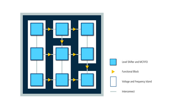
Figure 1: voltage and frequency island example
Clock input to the blocks is also segregated so that the clock frequency can be tuned as the voltage is adjusted. Each voltage and frequency ‘island’ can then be adjusted to provide the desired performance at the lowest possible supply load. Level shifters and synchronisation circuits such as mixed clock FIFOs (MCFIFOs) connect signals between different islands.
In order to make use of VFI, the application processor on the SoC implements DVFS algorithms to adjust voltage and frequency for each island. Parameters for voltage versus frequency performance are programmed offline and the DVFS algorithms use these parameters to make adjustments based on expected workload. Parameters for the DVFS algorithms can be generated using a combination of simulation and transient analysis.
SPICE-level analogue simulation tools such as the Cadence Spectre Circuit Simulator can improve DVFS algorithms by providing circuit characteristics based on silicon accurate device models. Precision results can highlight trouble spots before a design is committed to silicon. Algorithm parameters can be fine-tuned using post layout simulation. Statistical methods such as Monte Carlo analysis can further improve parameters by analysing multiple circuit variations.
Transient analysis is useful for developing DVFS parameters by predicting circuit performance over time and at varying loads. Thermal performance and power supply design can be improved by analysing circuit response to transient over and under voltages.
However, as more devices are incorporated on-chip, simulation and transient analysis become more difficult and time consuming. Device models become more complex at smaller geometries as once negligible effects become more significant. Interaction between circuit elements is dependent on layout, which increases the number of variables. All these additional elements require more time to analyse with existing simulators or more processing power to keep simulation time manageable.
Improving DVFS performance
DVFS algorithms based solely on expected workload make assumptions about circuit operation based on offline simulation and analysis. Process variations can degrade performance by causing identical circuits within a die to behave differently. Modeling the effects of process variations is difficult at best, leading to more conservative design margins.
Voltage monitoring IP can improve performance of DVFS algorithms without the need for complex simulation models. Process variation aware DVFS algorithms can use feedback from the voltage monitoring IP to ensure island supply voltage is at the correct level. If the voltage is incorrect, the control algorithm can increase or decrease the value sent to the programmable regulator to compensate for the difference. Sensors can be added to monitor circuit temperature, which can be used to extrapolate circuit performance. As the temperature of an island changes, clock frequency and voltage can be scaled to bring performance to the desired level.
Supply noise performance
Almost every high performance SoC has high data rate interfaces built into it for access to external memory, storage, peripherals or just for inter-chip communication. These interfaces are implemented in the form of standard high speed interconnect protocols (such as USB, PCIe, etc.) or in several cases, in the form of proprietary SerDes such as in high performance GPUs and server processors.
These SerDes can run at data rates in excess of 10Gbps with the actual performance in a lossy medium tightly coupled to the jitter budget allocated by the designers. Such high speed links are extremely sensitive to excess jitter contribution from any source. Power supply and ground noise has been established as a significant source of jitter in TX and RX signals as well as clock paths requiring significant mitigation efforts from the designers.
However, any robustness in the design usually comes at the cost of increased power and area. As a result, there is a clear benefit to minimising the noise created on supply and ground nodes inside the die. A lot of research effort is being directed toward modelling of the package and on-die parasitic loads so that the efficacy of power supply decoupling on-die and off-die can be studied.
However, thus far these are simulations, which can’t be correlated directly with silicon results. Once again, the utility of on-die measurement IP that provides the ability to measure high frequency noise on the die is beyond question. Such IP will allow the designers a peek into the robustness of the design and allow them to adjust the amount of ‘overdesign’ in the process.
Transient Voltage Monitoring IP
The Cadence Transient Voltage Monitoring IP addresses all the issues described here. The IP provides eight high resolution, high accuracy channels of analogue input - two high speed and six low speed channels. Additionally, a programmable comparator allows for very fast transient detection. A block diagram of the IP is shown in figure 2.
![]()
Figure 2: Cadence Transient Voltage Monitoring IP top level block diagram
All the channels boast 3mV sensitivity and 10mV accuracy over a 12-bit sample size. The two high speed channels support >1GHz sampling bandwidth, which provides the SoC with an ability to accurately monitor transient noise at several hundred MHz. By providing such high resolution, the IP can be used to tightly control supply variations in individual islands, thus optimising the SoC performance. The short sample period (~100ns) and 1MHz sample clock allow the IP to capture fast transients.
The IP features a programmable high speed comparator that responds to over and under voltage levels faster than the SAR ADC. Therefore, voltage transients that are too fast for the DVFS algorithm can be detected and appropriate action taken.
Armed with the Cadence Transient Voltage Monitoring IP, designers can once again have the upper hand in taking SoC design to the next level of performance.
Product Spotlight
APV1111GVY
Panasonic

Panasonic PhotoMOS® Photovoltaic MOSFET High-Power Drivers
| SKU: | |
|---|---|
| Stock: | 3490 |
| Cost: | $3.95 |
