
SiC epitaxial wafers feature low defect density
Showa Denko (SDK) has developed a new grade of SiC epitaxial wafers for power devices with very low defect density. This month, SDK will start commercial shipments of the recent grade, in 4 and 6" in diameter, under the trade name of 'High-Grade Epi' (HGE). When compared with the mainstream Si-based semiconductors, SiC-based power devices can operate under high temperature, voltage and current conditions, while substantially reducing energy loss.
These features enable the production of smaller, lighter and more energy-efficient next-gen power control modules. SiC power devices are already used as power sources of servers for data centers, distributed power supply systems for new energies and in subway railcars. Demand is expected to grow further as plans have been announced to use SiC power devices in vehicles.
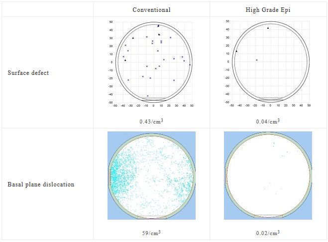
Furthermore, efforts are under way to develop SiC-based ultra-high-voltage (10KV class) devices for use in power generation/transmission systems. Power modules for high-voltage, high-current applications mainly contain devices with the structure of SBD (Schottky barrier diode) and transistors with the structure of MOSFET. While SiC is increasingly used in SBD, it is difficult to use SiC in MOSFET. As MOSFET's oxide film, formed on the surface of an epitaxial wafer, is used in device operations, finer Surface Defect (SD) and various types of crystal defects, including Basal Plane Dislocation (BPD), considerably affect the yield and product quality.
For automotive applications, meanwhile, large chips measuring around 10mm2 are made out of epitaxial wafers. This is because one device needs to handle a current as high as 100A. To prevent deterioration in the production yield of such large chips, the defect density of epitaxial wafers should be controlled within 0.1/cm2.
In the latest product HGE, SDK has succeeded in controlling the number of SD within 0.1/cm2 (one-third the current level of SDK's conventional product) and of BPD within 0.1/cm2. As a result, it is now possible to almost eliminate device defects attributable to BPD (assuming the use of a 10mm2 chip).
Using the HGE technology, SDK has also succeeded in producing SiC epitaxial wafers with film thickness of 100μm or more, having low levels of defect density and good uniformity. SDK will start commercial shipments of these SiC epitaxial wafers for use in power generation/transmission systems. The size of the market for SiC epitaxial wafers for power devices is expected to reach ¥100bn in 2025.
Product Spotlight
APV1111GVY
Panasonic

Panasonic PhotoMOS® Photovoltaic MOSFET High-Power Drivers
| SKU: | |
|---|---|
| Stock: | 3490 |
| Cost: | $3.95 |
