Power
NXP Introduces World’s First 2-mm x 2-mm MOSFETs with Tin-Plated Solderable Side Pads
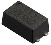
NXP Semiconductors today introduced the industry’s first MOSFETs in a 2-mm x 2-mm low-profile DFN package with tin-plated, solderable side pads. These unique side pads offer the advantage of optical soldering inspection, as well as a better quality of solder connection compared to conventional leadless packages.
##IMAvailable immediately, the new PMPB11EN and PMPB20EN 30V N-Channel MOSFETs are the first of more than 20 devices housed in the DFN2020MD-6 (SOT1220) package from NXP. Both MOSFETs have a maximum drain current (ID) of >10 A, and very low Rds(on) values of 12 mOhm typ and 16.5 mOhm typ at 10V respectively for reduced conduction losses, which enable lower power consumption and longer battery life.
Only 0.6 mm in height, the new DFN2020 MOSFETs are also thinner than most 2-mm x 2-mm products on the market today, making them ideal for ultra-small load switches, power converters, and charger switches in portable applications such as smartphones and tablets. The MOSFETs are also well suited for other space-constrained applications including DC motors, server and network communications, as well as LED lighting, where power density and efficiency are critical.
##IMAGE_2_C##
Eight times smaller than standard SO8 packages, DFN2020 offers comparable thermal resistance, and can replace many larger MOSFET packages such as SO8, 3x3 or TSSOP8 with the same Rds(on) value range.
The new MOSFETs enhance NXP’s ultra-small leadless MOSFET line-up which will include more than 60 types in 2-mm x 2-mm and 1-mm x 0.6-mm package sizes by the end of this year. NXP is now a major player in low Rds(on) MOSFETs in very small sizes, offering both FET and bipolar transistor technologies.


