
Bypassing MOSFETs can help avoid inefficiency
How bypass MOSFETs can help avoid the inefficiency incurred when using Schottky diodes in power supply ORing topologies. By Chew Lye Huat, Linear Technology.
Schottky diodes are used in a variety of ways to implement multi-source power systems. For instance, high availability electronic systems employ power Schottky diode-OR circuits in redundant power systems. Diode ORing is also used in systems with alternate power sources, such as an AC wall adapter and a backup battery feed. The problem is that the Schottky diodes consume power due to the forward voltage drop; the resulting heat must be dissipated with dedicated copper area on the PCB, or by heat sinks bolted to the diode, both of which require significant space.
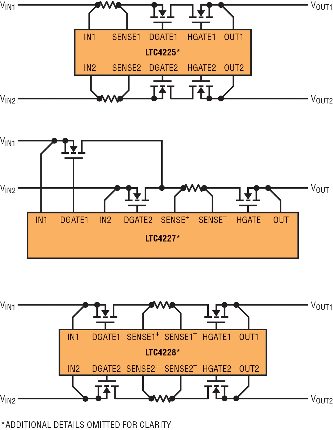
Figure 1 - An overview of different configurations with sense resistor and external N-channel MOSFETs for the LTC4225, LTC4227 and LTC4228
Using external N-channel MOSFETs can minimise the voltage drop from the supply to the load when the MOSFETs are turned on. When an input source voltage drops below the output common supply voltage, the appropriate MOSFET is turned off, thereby matching the function and performance of an ideal diode. As shown in Figure 1, by adding a current sense resistor and configuring two MOSFETs back-to-back with separate gate control, the LTC4225 enhances the ideal diode performance with inrush current limiting and overcurrent protection. This allows the boards to be safely inserted and removed from a live backplane without damaging the connector. The LTC4227 can be used with the current sense resistor and the Hot Swap MOSFET added after the parallel-connected ideal diode MOSFET to save one MOSFET. By configuring the sense resistor between the ideal diode and Hot Swap MOSFET, the LTC4228 improves on the LTC4225 by recovering more quickly from input brownouts to preserve the output voltage.
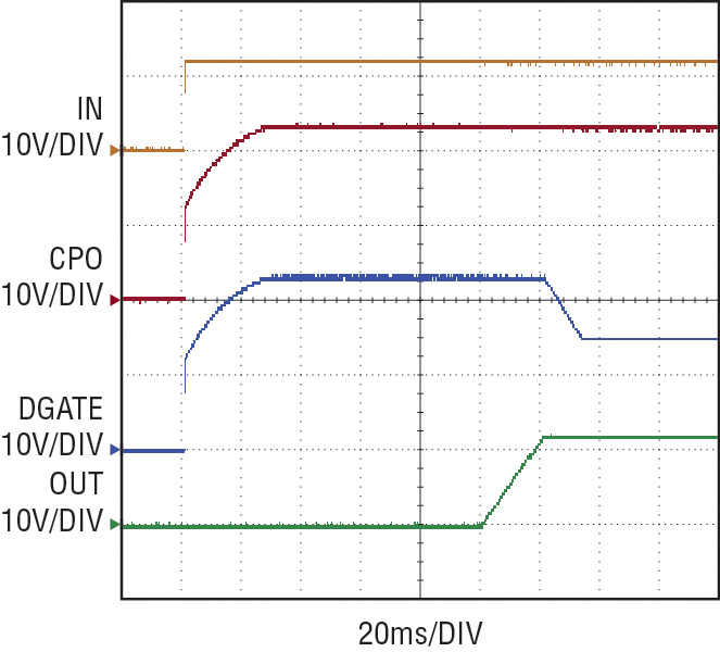
Figure 2 - Ideal diode controller CPO and DGATE pull up when IN supply turns on
Ideal diode control
Devices like this function as an ideal diode by monitoring the voltage between IN and OUT pins with an internal gate drive amplifier. The amplifier quickly turns on the MOSFET for ideal diode control when it senses a large forward voltage drop (Figure 2). An external capacitor provides the charge needed to quickly turn on the ideal diode MOSFET, typically primed at power-up using an internal charge pump. In this case, if the load current causes more than 25mV of voltage drop, the gate voltage rises to enhance the MOSFET used for ideal diode control. In the event of an input supply short-circuit when the MOSFETs are conducting, a large reverse current starts flowing from the load toward the input. The gate drive amplifier detects this failure condition as soon as it appears and turns off the ideal diode MOSFET.
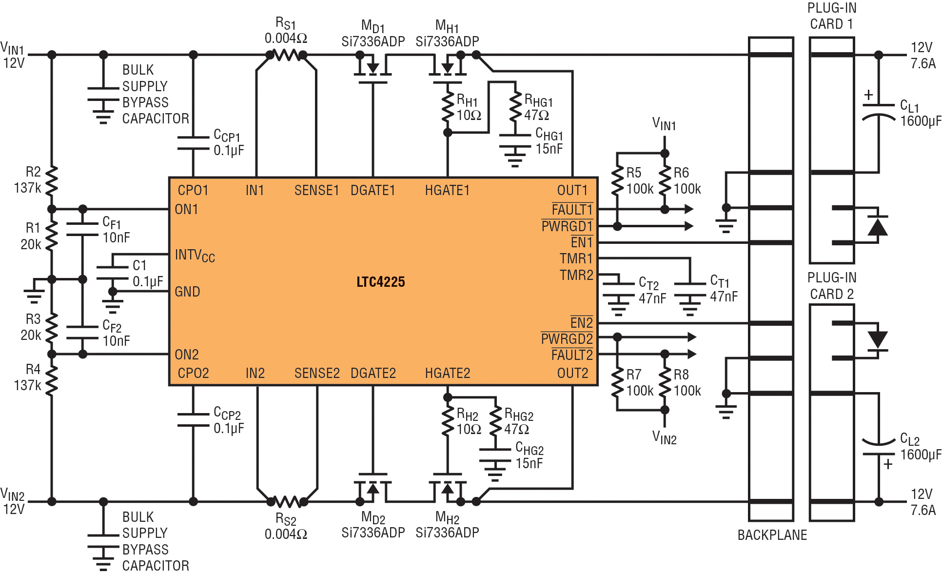
Figure 3 - The LTC4225 in a µTCA application to supply 12V power to two µTCA slots
In a typical application with redundant supplies (Figure 3), the outputs are diode-ORed at the backplane, so cards can be removed or inserted without powering down the system. If the main supply loses power, the controller reacts quickly to turn off the ideal diode MOSFET in the main supply path and turn on the MOSFET in the redundant supply path, providing a smooth supply switchover to the output load. The Hot Swap MOSFETs remain on so they do not affect the supply switchover. The controller turns off a Hot Swap MOSFET when the respective ON pin is pulled low or EN pin is pulled high. When an overcurrent fault is detected at the output, the gate of the Hot Swap MOSFET is pulled down quickly, after which the output is regulated in current limit until the fault filter delay set by the TMR pin capacitor times out. The Hot Swap MOSFET is turned off and the FAULT pin is latched-low to indicate a fault. The electronic circuit breaker is reset by pulling the ON pin below 0.6V.
Prioritising a power supply
In a traditional diode-ORed multi-supply system, the input supply with the higher voltage is passed to the output, while the lower voltage supply is shut out. This simple solution satisfies the needs of applications where the priority of the supplies is not simply a matter of the higher voltage supply winning. Figure 4 shows a backup supply system where the 5V primary supply (INPUT1) is passed to the output whenever it is available, while the 12V backup supply (INPUT2) is called on only when the primary supply fails to deliver.
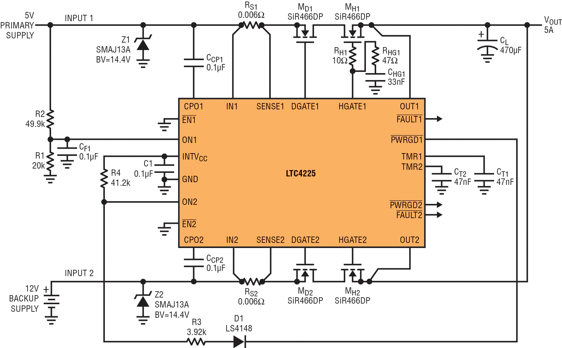
Figure 4 - LTC4225 for 2-channel power prioritiser with IN1 as the prioritising input
As long as INPUT1 is above the 4.3V UV threshold set by the R1-R2 divider at the ON1 pin, MH1 is turned on, connecting INPUT1 to the output. When MH1 is on, PWRGD1 goes low, which in turn pulls ON2 low and disables the IN2 path by turning MH2 off. If the primary supply fails and INPUT1 drops below 4.3V, ON1 turns off MH1 and PWRGD1 goes high, allowing ON2 to turn on MH2 and connect the INPUT2 to the output. The ideal diode MOSFETs MD1 and MD2 prevent backfeeding of one input to the other under any condition.
The LTC4225 allows applications with back-to-back MOSFETs to be configured with the MOSFET on the supply side as the ideal diode and the MOSFET on the load side as the Hot Swap control, or vice versa. In Figure 5, an external Zener diode clamp may be required between the GATE and SOURCE pins of the MOSFET to prevent it from breaking down if the MOSFET’s gate-to-source voltage is rated for less than 20V. In either arrangement, LTC4225 smoothly switches between supplies with its ideal diode ORing between the IN and OUT pins.
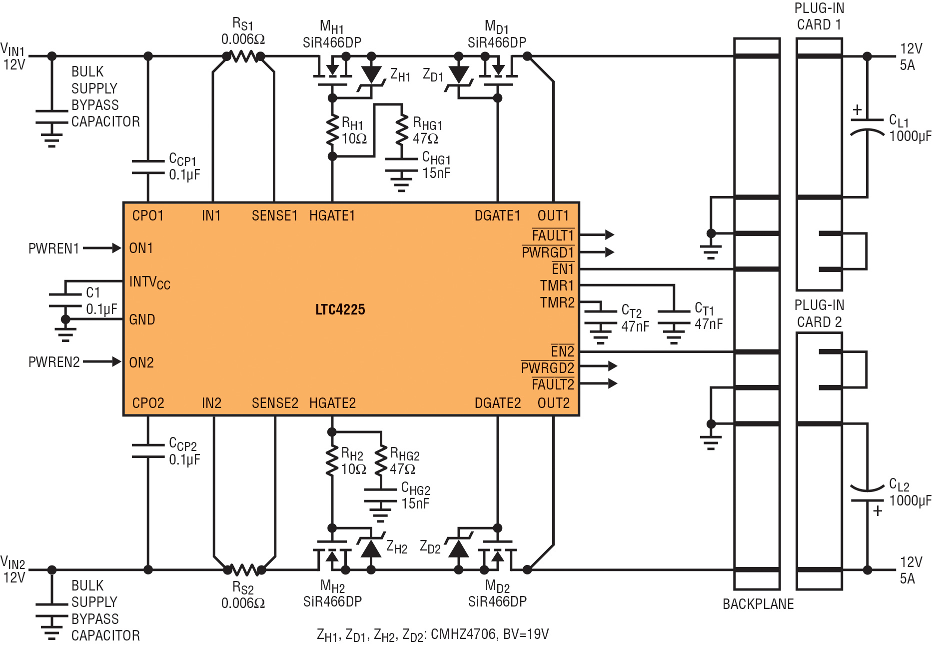
Figure 5 - LTC4225 for application with the Hot Swap MOSFET on the supply side and the ideal diode MOSFET on the load side
In the application shown in Figure 3, if one of the input supplies collapses to ground momentarily while the other supply is not available, HGATE is pulled low to turn off the Hot Swap MOSFET as the IN supply drops below the undervoltage lockout threshold. When the input supply recovers, HGATE is allowed to start up to turn on the MOSFET. As it takes a while to charge up HGATE and the depleted output capacitance, the output voltage may brown out during this period. In this situation, the LTC4228 offers an advantage over the LTC4225 by recovering more quickly to preserve the output voltage.
Several devices exist today that enable ideal diode and Hot Swap functions for two power rails by controlling external N-channel MOSFETs. They feature fast reverse turn-off, smooth supply switchover, active current limit and status and fault reporting. Their tight 5% circuit breaker threshold accuracy and fast acting current limit protect the supplies against overcurrent faults.
Product Spotlight
APV1111GVY
Panasonic

Panasonic PhotoMOS® Photovoltaic MOSFET High-Power Drivers
| SKU: | |
|---|---|
| Stock: | 3490 |
| Cost: | $3.95 |
