
Affordable, accessible SiC devices
Rethinking wafer fabrication and converter design can make SiC devices more affordable and accessible, advocate Corey Deyalsingh, Littelfuse and Sujit Banerjee, Monolith Semiconductor
Silicon carbide (SiC) is a rapidly emerging semiconductor material that lets power devices operate at higher switching and higher temperatures with lower losses than conventional silicon. It allows inverters and other energy conversion systems to be built with significantly improved power density, energy efficiency and cost.
Global energy consumption is growing, highlighting the importance of developing clean (non-fossil fuel) technology and boosting energy- efficiency. SiC represents one important way to advance the clean energy revolution. At the same time, the need for grid energy storage to balance fluctuations in energy generated by technologies like wind and solar power is also growing. SiC technology makes that possible cheaply, compactly, and efficiently through the use of conversion electronics connected to energy storage systems.
Demand for hybrid and electric vehicles (EVs) makes energy-efficient power conversion electronics critical to extend range. SiC devices allow the design of smaller, lighter, more rugged and more efficient onboard power conversion systems for traction inverters, DC/DC converters, on-board charging.
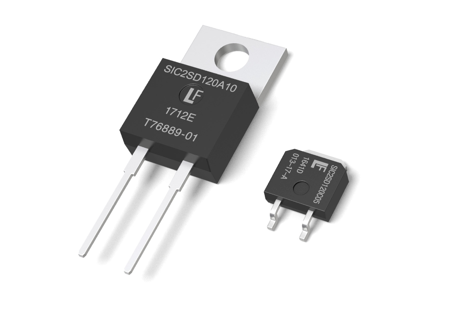 Figure 1: LSIC2SD120 1200V SiC Schottky diodes are available with current ratings from 5.0 to 10A in TO-220-2L or TO-252-2L packages
As more information is stored in the cloud, data centres will consume a growing percentage of the energy produced. SiC technology will also be vital to increasing power density while increasing efficiency and reducing operating costs.
Today, however, relatively few SiC discrete devices (at least, SiC MOSFETs) are commercially available. Few suppliers have stock available for purchase, which limits widespread adoption and slows entry to the mainstream. To encourage SiC adoption, suppliers must take steps to improve confidence in the availability of qualified SiC devices. They must also be willing to work in co-operation with smaller, emerging customers to help them apply the emerging technology. In particular, suppliers need to take into account the needs of customers who do not represent volume business immediately but have the potential for growth.
Partnering to fulfil SiC's promise
Littelfuse first invested in Monolith Semiconductor, a technology company developing SiC technology, in December 2015, to help bring SiC devices into the mainstream. It now holds a majority ownership position in Monolith which leverages a fabless model to manufacture SiC devices in a high-volume, automotive-qualified, 150mm CMOS fab. Existing fab processes and tools are reused wherever possible and SiC wafers are run in parallel with existing silicon CMOS production. This manufacturing approach reduces manufacturing costs at lower volumes for price-competitive entry into the SiC market. Not having the cost of building and operating a fab is central to being agile and maintaining a low-cost structure, maintains Littelfuse. It also accelerates time to market, enables faster ramp-up and improves device quality.
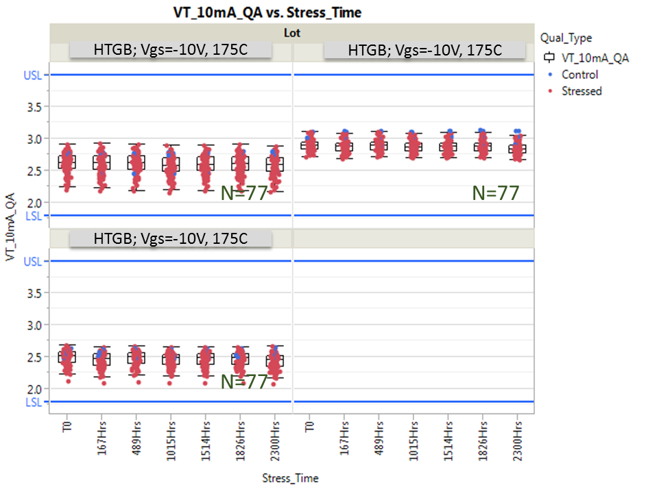
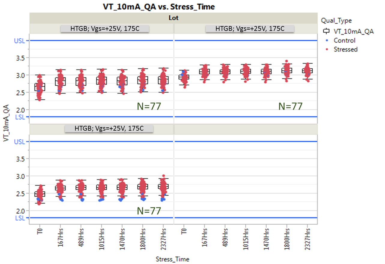 Figure 2a: Negative, VGS = -10 V, and (Figure 2b) positive, VGS = 25 V, high-temperature gate bias (HTGB) stress tests performed at 175°C on 77 devices from three wafer lots out to 2300 hours showed negligible deviation
In automotive-qualified fabs, statistical process control (SPC) monitoring of the fabrication process, materials inspections, wafer level reliability (WLR) testing, reliability monitoring, and strict change control management ensure quality. Littelfuse-Monolith SiC MOSFETs provide five to 10 times reduction in terms of switching losses compared to silicon IGBTs. In a recent power converter demonstration, these 1200V MOSFETs had the highest efficiency, comparable to the best-performing SiC MOSFET available on the open market.
What SiC brings to Schottky diodes
SiC has a high thermal conductivity, and temperature has little influence on its switching and thermal characteristics. Over the last 20 years, SiC Schottky diodes have become available with increasingly higher voltage ratings. SiC Schottky diodes have approximately 40 times lower reverse leakage current than PN silicon Schottky diodes. The LSIC2SD120 series 1200V SiC Schottky diodes (Figure 1) are the partnership's first product introduction. The diodes are designed to reduce switching losses dramatically and enable substantial increases in system efficiency and robustness.
The diodes are claimed to provide best-in-class capacitive stored charge and negligible reverse recovery to ensure low switching losses in high-frequency power switching and reduced stress on the opposing switch. Low forward voltage drop allows for reduced conduction losses. A maximum junction temperature of 175°C provides for a larger design margin and relaxed thermal management requirements. Their merged PN-Schottky (MPS) architecture enhances surge capability and ensures extremely low leakage, adds the company.
Applications include boost diodes in power factor correction, switch-mode power supplies, uninterruptible power supplies, solar inverters, industrial motor drives, EV charging and power conversion.
Longer lifetimes and lower costs
The quality of commercially available 1200V SiC MOSFETs has improved dramatically in recent years: channel mobility has risen to suitable levels, oxide lifetimes have reached an acceptable level for most mainstream industrial designs, and threshold voltages have become increasingly stable.
For example, accelerated time-dependent gate oxide breakdown (TDDB) testing performed at the National Institute of Standards and Technology (NIST) has predicted an oxide lifetime of more than 100 years, even at junction temperatures above 200°C, for Monolith Semiconductor's MOS technology. The acceleration factors of applied electric field across the oxide were taken to more than 9MV/cm and junction temperature to 300°C. For reference, oxide electric fields used in practice are around 4MV/cm, with junction temperatures typically below 175°C. It is also worth noting that although temperature-dependent acceleration factors are commonly seen in silicon MOS, they have not been seen by NIST for SiC MOS prior to working with the devices from Monolith.
The threshold voltage stability of these MOSFETs has also been demonstrated. High-temperature gate bias (HTGB) testing was performed at a junction temperature of 175°C and under negative (VGS = -10 V) (Figure 2a) and positive (VGS = 25 V) (Figure 2b) gate voltages.
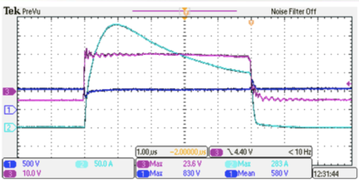
Figure 3: Short-circuit testing of a 1200V, 80m SiC MOSFET at a DC link of 600V and VGS = 20V, indicates a withstand time of at least 5.0microseconds
The blocking voltage and off-state leakage of the MOSFETs has proved to be stable long term, based on high temperature reverse bias (HTRB) reliability testing results. For device ruggedness, preliminary measurements reveal a short-circuit withstand time of at least five microseconds and an avalanche energy of 1J (Figure 3).
Even if SiC MOSFETs remain more expensive than comparable silicon (Si) IGBTs, designers are already seeing system-level price benefits of using them rather than Si IGBTs at today's price levels, perhaps even using SiC discrete devices rather than more expensive IGBT modules. SiC MOSFET pricing is likely to become increasingly competitive as economies of scale take hold, with 150 mm wafers and the rest of the SiC supply chain.
Tools to maximise performance
Obtaining the maximum performance from high-voltage SiC MOSFETs and diodes requires more than just plugging them into an application. For example, it requires access to a characterisation board designed for use with SiC devices that has minimal parasitic inductances and supports precise measurement of voltage and current waveforms. It also calls for careful and optimised gate drive design and layout to minimise noise coupling. The Monolith–Littelfuse Dynamic Characterization Toolkit (Figure 4) allows designers to characterise the switching behaviour of SiC devices accurately and explore optimised driving via gate driver parameter tuning.
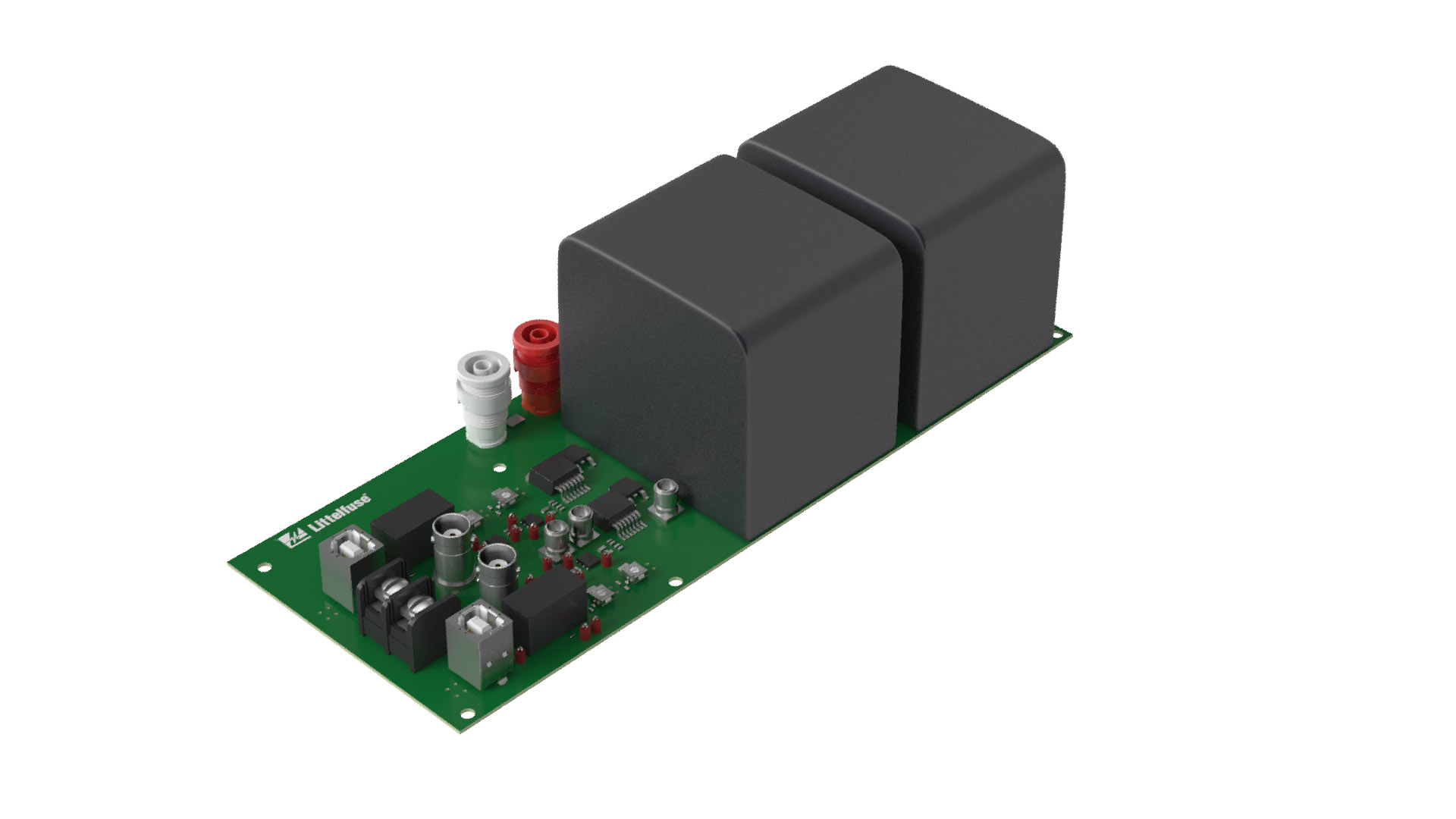
Figure 4: The Dynamic Characterization Toolkit allows for precise voltage and current waveforms measurements
The Littelfuse-Monolith 5kW Evaluation Converter (Figure 5) is designed to accelerate the power converter design and layout process. Using a modular design strategy and components with similar footprints, it provides a versatile and adaptable platform for converter-level testing.
After decades of development effort, it is increasingly clear that SiC diodes and MOSFETs are finally coming into their own and are poised for widespread commercial success and a substantial role in the green energy movement.
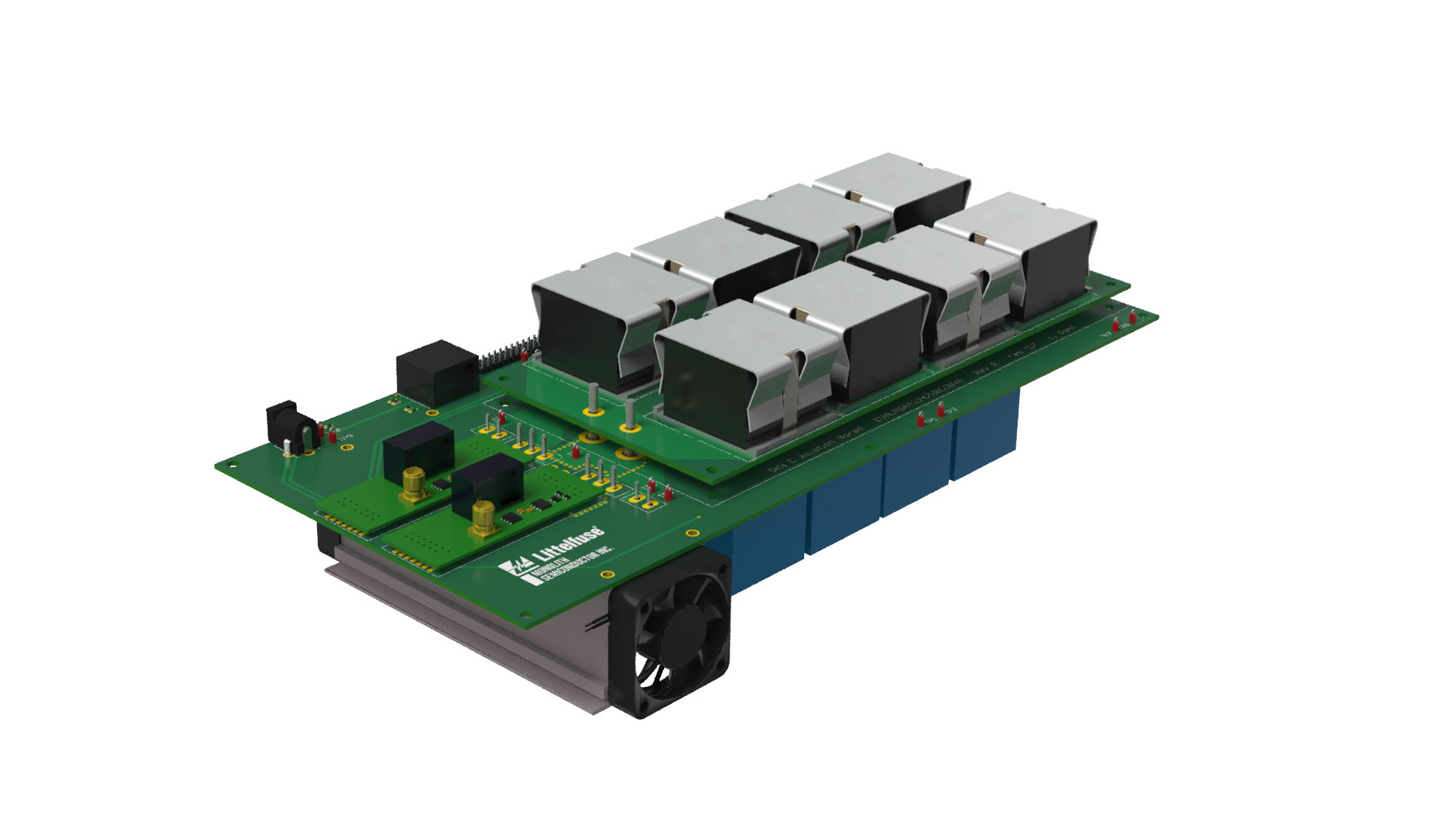 Figure 5: The 5kW Evaluation Converter accelerates power converter design and layout process
Product Spotlight
APV1111GVY
Panasonic

Panasonic PhotoMOS® Photovoltaic MOSFET High-Power Drivers
| SKU: | |
|---|---|
| Stock: | 3490 |
| Cost: | $3.95 |
