
Protecting patients and their medical equipment
Today, patients rely on a growing number of portable medical devices such as glucose meters, blood pressure monitors or defibrillators. But even a seemingly minor electrostatic discharge could easily render a portable medical device useless. To ensure safe, reliable performance of these devices, their designers should use best practices to factor in circuit protection requirements from the earliest stages of the circuit design process. By James Colby, Manager, Business and Technology Development, Semiconductor Business Unit, Littelfuse.
Multiple aspects of a medical instrument’s circuitry are subject to a variety of electrical threats over its lifetime. In short, any power or communication interface represents a potential gateway for an electrical transient that would make it susceptible to damage over the lifetime of the device. To help avoid any danger to the patient, it is essential for circuit designers to pay attention to a wide range of circuits including the power supply (battery pack, DC input, AC input), microprocessor, audio/speaker lines, communication interfaces (wired and wireless), sensors, LCD displays, keypads, and buttons. Therefore, it is strongly recommended that Design Engineers weigh circuit protection options as early as possible during the board layout process. They will need to keep in mind both the optimal protection device and the optimal location for use with a particular chipset.
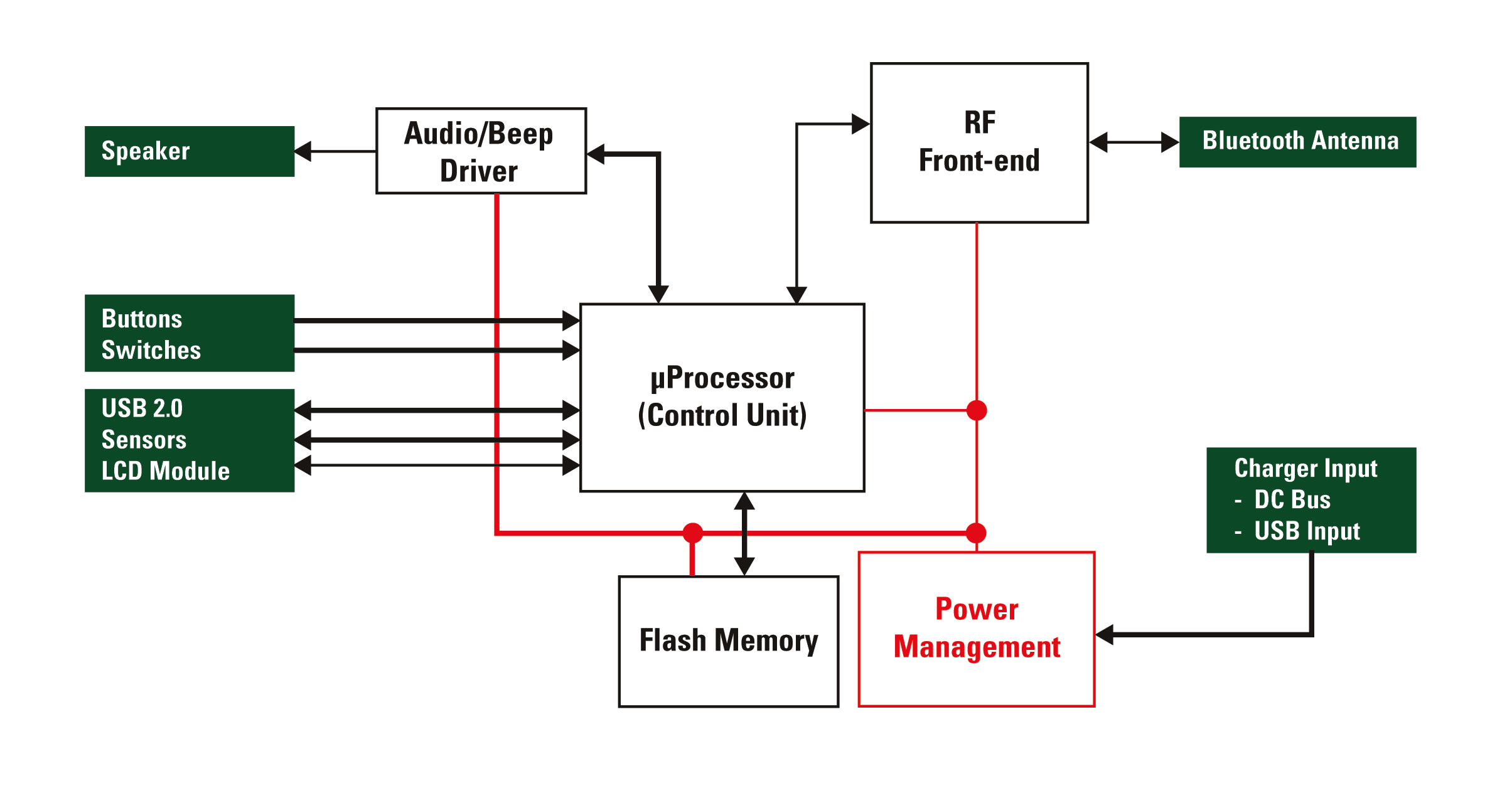
Figure 1 - Electrical block diagram of a generic portable medical device
Figure 1 is a simplified electrical diagram representing a handheld medical device (e.g. blood glucose meter, heart rate monitor) with the green boxes indicating circuits that may be susceptible to overvoltage or overcurrent conditions. Because both patients and healthcare providers will handle this device frequently, the predominant electrical threat is a simple static discharge. An electrostatic discharge (ESD) event can transfer excessive voltage and current to internal circuitry.
First lines of defence
To ensure the security and integrity of patient data, protecting the communication interfaces of medical devices is a high priority. The Continua Health Alliance’s Design Guidelines define specific versions of Bluetooth and USB interfaces that act as wireless and wired transports to link health care instruments with caregivers. The following examples illustrate how various protection devices might be applied for portable equipment.
As illustrated in Figure 2 (top), a handheld instrument’s wireless (RF) interface can be exposed to ESD surges induced through its antenna. This circuit shows a semiconductor-based solution that protects the RF amplifier input module of the Bluetooth circuit from ESD threats. The protection device is a 0.5pF (to maintain signal integrity) discrete diode that provides low clamping voltage to protect the equipment’s sensitive RF front-end.
, Protection of the sensor measurement circuit (bottom).jpg)
Figure 2 - Bluetooth antenna and RF front-end protection (top), Protection of the sensor measurement circuit (bottom)
An instrument’s sensor input (such as the input that connects a test strip for a glucose meter to its controller IC) is the interface between the user and the measurement circuitry. This input also makes an instrument susceptible to ESD damage because the sensor makes contact with the user in some fashion. As shown in Figure 2 (bottom), several discrete diodes can be used in this circuit (four lines are shown here). These devices offer low clamping voltage, as well as extremely low leakage current (less than 100nA) and can ensure the sensor circuit receives a strong enough signal to produce an accurate measurement.
Many medical product designers use the product’s USB port as both an input for recharging the on-board battery and as a way to transfer data. As a result, this port can inadvertently act as a gateway for ESD and overload currents. Furthermore, the ESD protection used in previous generations of USB may be incompatible with the newest version (USB 3.0) due to the increase in data transfer rate to 5Gbps and required decrease in channel capacitance in order to support the new data rate. As a result, designers are more challenged to find voltage transient protection solutions that can protect sensitive data lines without adding signal distorting capacitance.
The additional data pairs of USB 3.0 expose electrical systems to greater ESD threats because it provides more possible entryways for the electrical transients. New silicon array ESD protection devices, which are designed to be placed directly on the data pairs, not only protect legacy USB 2.0 data lines but also these additional data signal pairs. For example, the Littelfuse SP3012 series TVS Diode Array (SPA Diode) integrates either four or six channels of ultra-low capacitance rail-to-rail diodes and an additional zener diode to provide protection for medical devices that may be subject to ESD. They are designed to absorb repetitive ESD strikes above the maximum level specified in the IEC61000-4-2 international standard (±8kV contact discharge) safely and without performance degradation. The extremely low loading capacitance (0.5pF) also makes it ideal for protecting high-speed signal lines.
.jpg)
Figure 3 - Protection of USB circuit (charging circuit and I/O)
Figure 3 offers an example of how to combine technologies to provide a more complete circuit protection solution for the legacy USB 2.0 port. First, a resettable PTC is used to protect against overcurrent conditions, in this case, a very low resistance device in a compact 0805 surface-mount package. This characteristic ensures that power dissipation and voltage drop are minimised when the device is being charged. Second, the power port and the I/O lines should be protected against ESD. This figure illustrates an array that protects all three lines and has a capacitance value low enough to ensure there is no data loss during high-speed (480Mbps) data transmission.
During regular use of a medical device, users make contact with the on/off switch and various other buttons frequently. Space-efficient diodes in an 0201 package can protect these controls. These diodes are extremely robust against ESD (up to 30kV contact discharge) and their small form factor allows them to be easily incorporated into the circuit board design. The discrete form factor also offers the board designer high layout flexibility.
The previous circuit protection examples highlighted some considerations for portable medical equipment. For higher-end equipment (imaging, diagnostic, lab), additional protection devices are relevant because this equipment is much more complicated and is exposed to a greater number of electrical threats.
Product Spotlight
APV1111GVY
Panasonic

Panasonic PhotoMOS® Photovoltaic MOSFET High-Power Drivers
| SKU: | |
|---|---|
| Stock: | 3490 |
| Cost: | $3.95 |
