
Paying for the right protection
Once aware of the danger, design engineers can easily help reduce the risk of chip damage caused by user-induced overvoltage transients, such as ESD. By Phillip Havens, Principal Engineer, Littelfuse, and Chad Marak, Director of Technical Marketing and TVS Diode Array Products, Semiconductor Business, Littelfuse.
Many consumers are oblivious to the fact that they, themselves, pose the single biggest risk to the electronic devices they use everyday. Circuit protection is a feature of all electronic devices - whether in cars, at home, or at work - because whenever humans touch any device containing sensitive electronic semiconductors, they can give rise to an ESD (electrostatic discharge) event.
If the surrounding air is particularly dry, because it’s a really hot or freezing cold day for example, just sliding from behind the steering wheel of a car can deliver a shocking jolt when touching the metal of the car door. While the jolt will have been no more than a nuisance to the driver, the effect may be much greater for sensitive electronic equipment. Imagine picking up a smartphone or tablet PC, only to find that some of the buttons or data ports are no longer working properly; these and other real-life headaches could be the direct result of that same jolt being injected into the device rather than the metal body of the car.
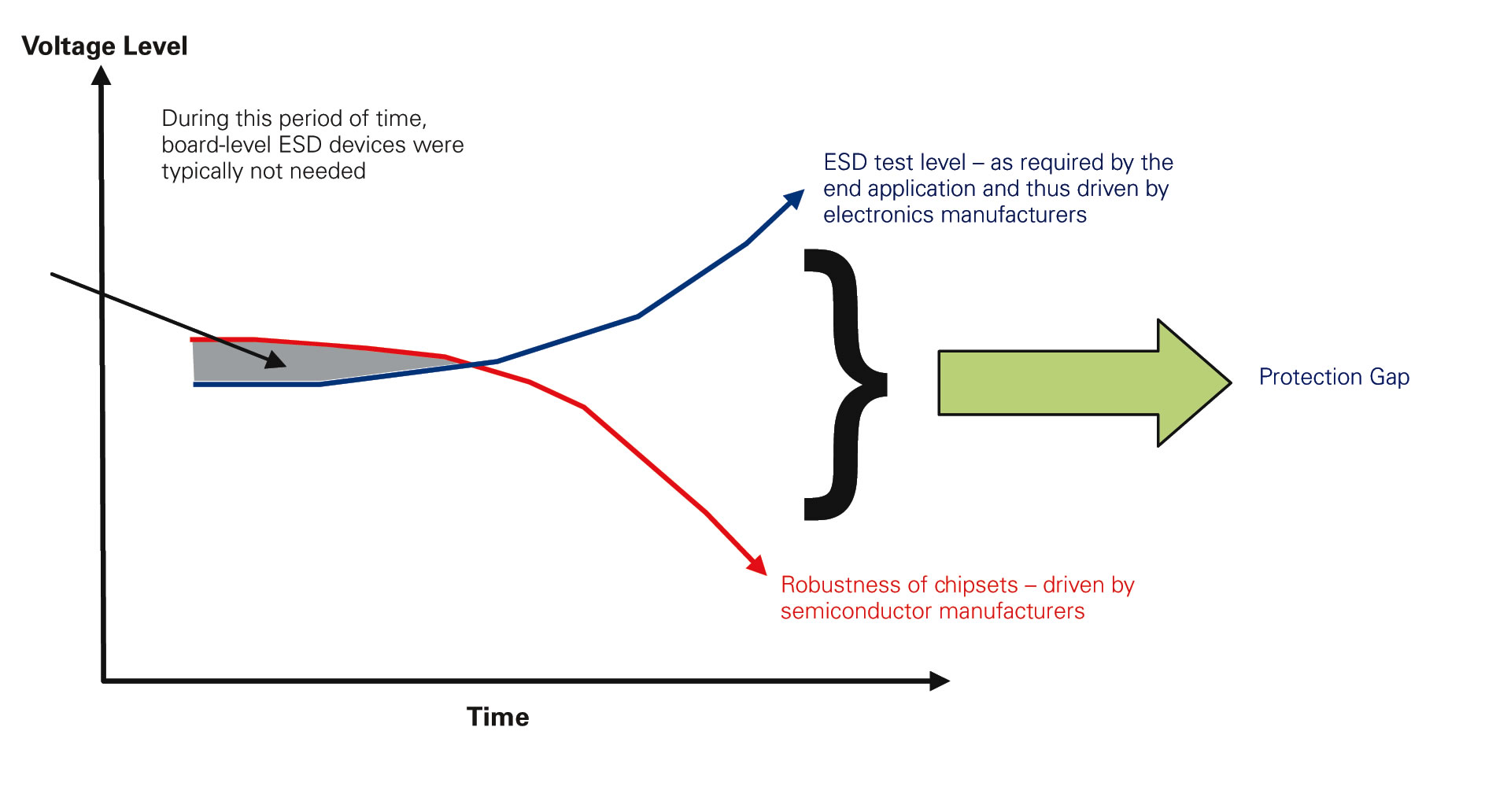
Figure 1: ESD testing
Even though ESD may not cause catastrophic events such as cell phones ‘exploding’, in the absence of ESD protection it might well prevent a cell phone from responding to any keypad or button inputs. Similarly, ESD damage can cause an interface port such as USB or Ethernet to no longer function properly when it is connected to other devices.
The physics behind ESD
These ESD events can all be traced back to a phenomenon known as triboelectric charging, which occurs when two materials make contact and then are quickly separated. As electrons are transferred between the two materials, one of them builds up positive charge and the other negative charge; the charge generates depends on several factors, including contact area, speed of separation, relative humidity and the chemistry of the materials. Although the process occurs thousands of times every day, it generally goes unnoticed except when the discharge is enough to cause someone mild, brief discomfort, such as walking across a carpet and grasping a door handle. The charge generated can range from hundreds of volts to tens of thousands of volts. Some examples of electrostatic generation are shown in Table 1.
Given the ongoing miniaturisation of silicon geometries via wafer processing, exposure to ESD events has become a real problem for today’s sophisticated yet cost-sensitive consumer electronics. Structures that offer protection against ESD are now too large and costly relative to the silicon integrated circuits (ICs) themselves to be included in the IC package. The result is that IC suppliers have removed or greatly reduced built-in ESD protection; the problem is that once these ICs are installed in consumer products and leave the controlled environment in which they were manufactured, they may well be subjected to uncontrolled ESD events.
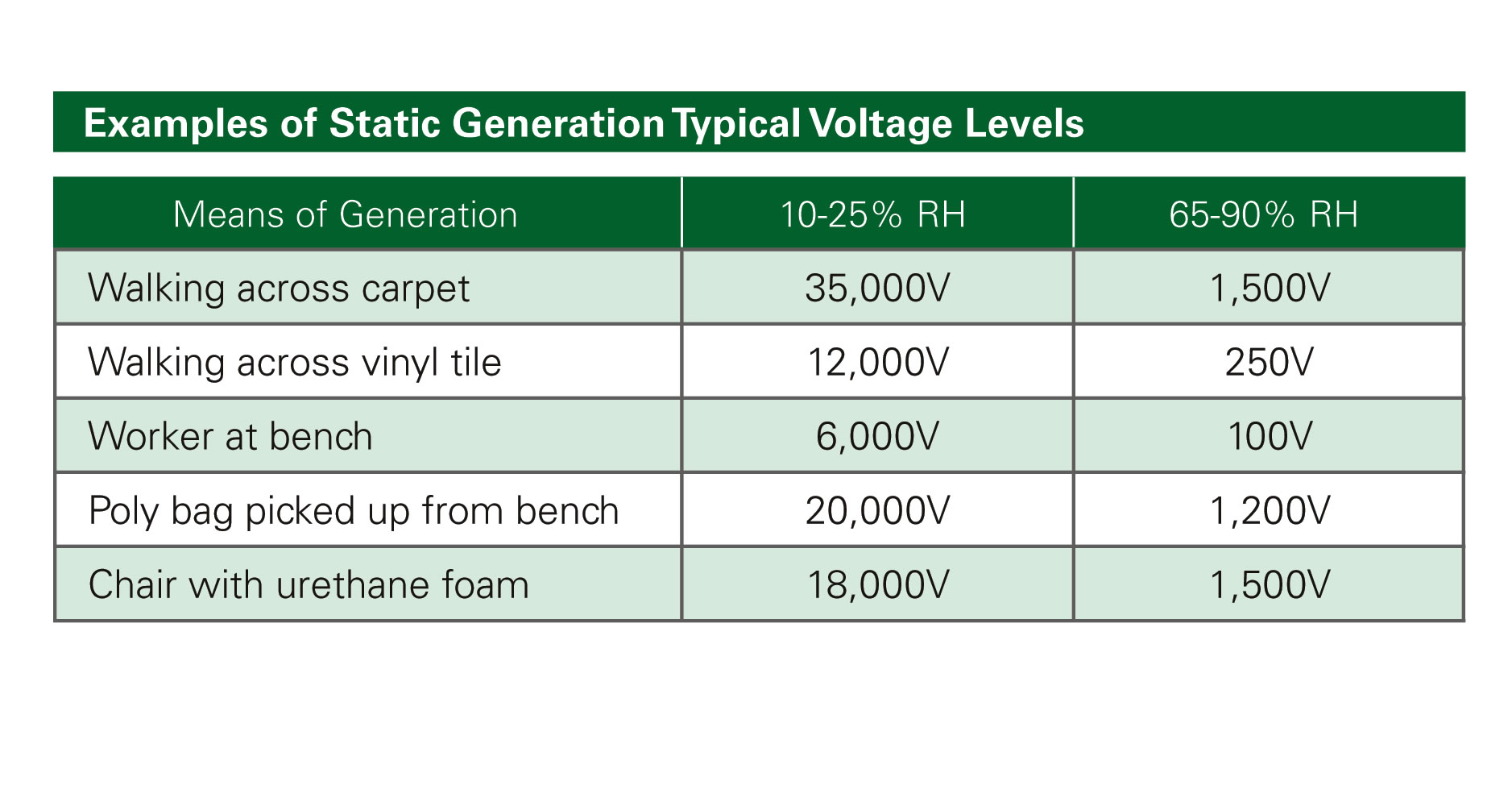
Table 1: ESD generation
What’s more, while IC manufacturers have historically used an ESD test model (MIL-STD-883, Method 3015: Human Body Model) that relates specifically to a manufacturing environment, equipment manufacturers — who are concerned with ESD events in the field — have used a harsher model as defined by the IEC (International Electrotechnical Commission), namely the IEC 61000-4-2 standard. As of this writing, most IC suppliers test their products at 500V with the Human Body Model (HBM), while end-user equipment manufacturers will test at 8000V (and beyond) using the IEC 61000-4-2 standard.
Table 1 compares the HBM (Human Body Model) ESD currents used by many chipset providers against the environmental ESD events outlined in IEC 61000-4-2 that many consumers will unknowingly inject into their consumer devices:
It is clear that the worst-case HBM ESD peak current is much lower than the worst-case ESD peak current under IEC 61000-4-2 (see the figures highlighted in red in Table 2). Compared to the 8kV event described in the HBM, the 8kV event under IEC 61000-4-2 implies a current that is 5.6 times greater. A chipset that survives HBM testing — as employed in the manufacturing environment — is not guaranteed to survive in the field, where the ESD exposure will be much more severe. Finally, as mentioned earlier, the majority of IC suppliers test only to 500V using the Human Body Model. If exposed to an 8kV ESD transient voltage in the field, a chipset will experience a near 100-fold increase in current; unless the IC design includes ESD protection, this level of current is more than enough to seal the chipset’s fate.
In recent years, application testing requirements have been tightened again and again, such that an ESD event of 8kV is typically the lowest level now used. Testing levels are trending towards 20kV and even 30kV, but at the same time IC suppliers have continued to remove protection from chipset designs to free up silicon area for more functionality. The following figure shows the gap between chipsets’ built-in ESD robustness and likely ESD exposure levels in field applications, highlighting the growing need for supplementary ESD protection.
Protection is crucial
If consumer electronics are to survive an ESD event and continue to function as originally designed, it is absolutely crucial to select the correct ESD protection device — typically referred to as a transient voltage suppressor (TVS) diode array. Dynamic resistance is one of the key ESD protection parameters to consider, perhaps even the most important when selecting a protection component. Any protection solution has an intrinsic resistance value associated with its clamping voltage characteristic. Ideally, intrinsic resistance is minimised to ensure that the protection solution has the lowest impedance path to ground during a surge event.
Figure 2: A protected IC
The schematic diagram in Figure 2 describes this issue. During an ESD event, the clamping device will turn on, going from its nominal state of high impedance to one of low impedance. If its series resistance is high, a high voltage (V = IR) will develop across the component, which means it offers the IC less effective protection. If its series resistance is low, the voltage that develops across the protection component will also be lower, in turn lowering the IC’s exposure level. This lower dynamic resistance (the protection component’s resistance value during clamping mode) allows more of the surge current to be routed away from the IC and to ground, as depicted in Figure 2. Littelfuse TVS diode arrays are designed to attain the lowest dynamic resistance value, thus minimising the overall voltage drop across the protection component and maximising the current that passes through it instead of through the protected IC.
In general, silicon protection devices provide the best ESD protection thanks to their inherently lower dynamic resistance compared to competing technologies such as polymers or ceramics. The typical dynamic resistance of silicon components ranges from 0.2Ω to 3.0Ω, depending on the supplier, while ceramic solutions (with an equal capacitance) offer dynamic resistances in the range of 2Ω to 5Ω on average.
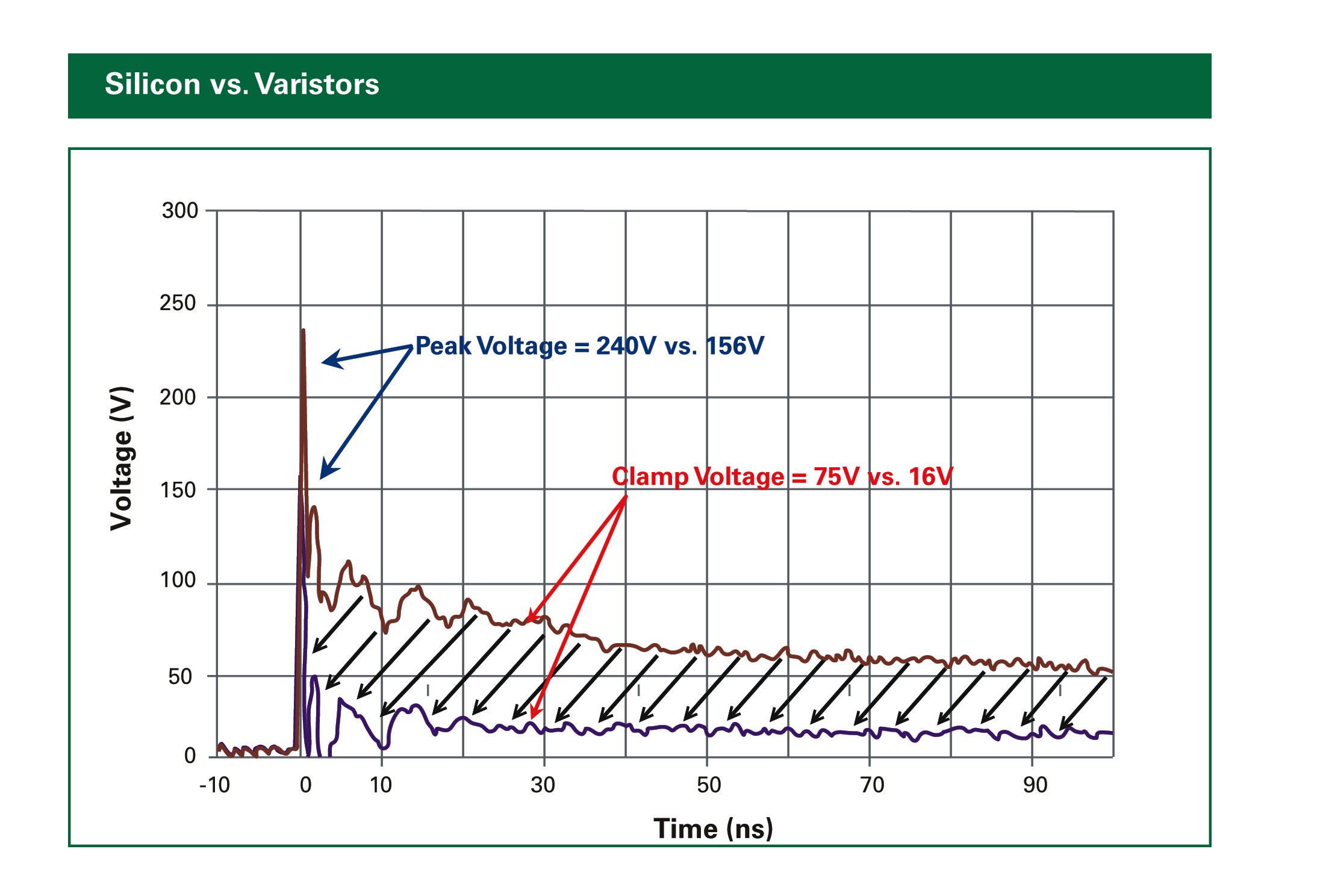
Figure 3: Silicon vs Varistors
The graph in Figure 3 shows the difference in let-through energy between a silicon component and its varistor counterpart when an 8kV ESD transient is injected into each component. It highlights the difference in leading-edge turn-on and in final clamping voltage. The area between the curves (the arrows) represents the difference between the two components in terms of how much energy the IC or chipset must be able to survive in order to prevent potential damage or premature failure.
Protection through standards
There seems to be no end to the range and constant evolution of consumer electronics: LCD TVs, smartphones, tablets, eReaders, set-top boxes, gaming consoles, digital cameras, audio players, and many more. But despite this variety, the devices commonly feature the same ports, or interconnects. As the device’s interface to the outside world, these interconnects require protection against ESD. Nearly all consumer products share some of the following functions:
- AC input/output
- DC input/output
- Battery pack
- Keypads/push buttons
- Video signals (HDMI, S-Video, composite video, LCD module)
- Audio output
- Low-speed data interface (USB1.1, IEEE 1394, RS 232C, RS 485)
- High-speed data interface (USB2.0, USB3.0, 10BaseT, 100BaseT, 1000BaseT)
- CATV/RF input/output
Some of these functions have to demonstrate compliance with national safety standards, which means they need overcurrent and overvoltage protection. Other functions may need protection from environmental factors such as ESD, but also nearby lightning surges or EFT (electrically fast transients) caused when nearby equipment with a high inductive load cycles on and off (e.g. a vacuum cleaner).
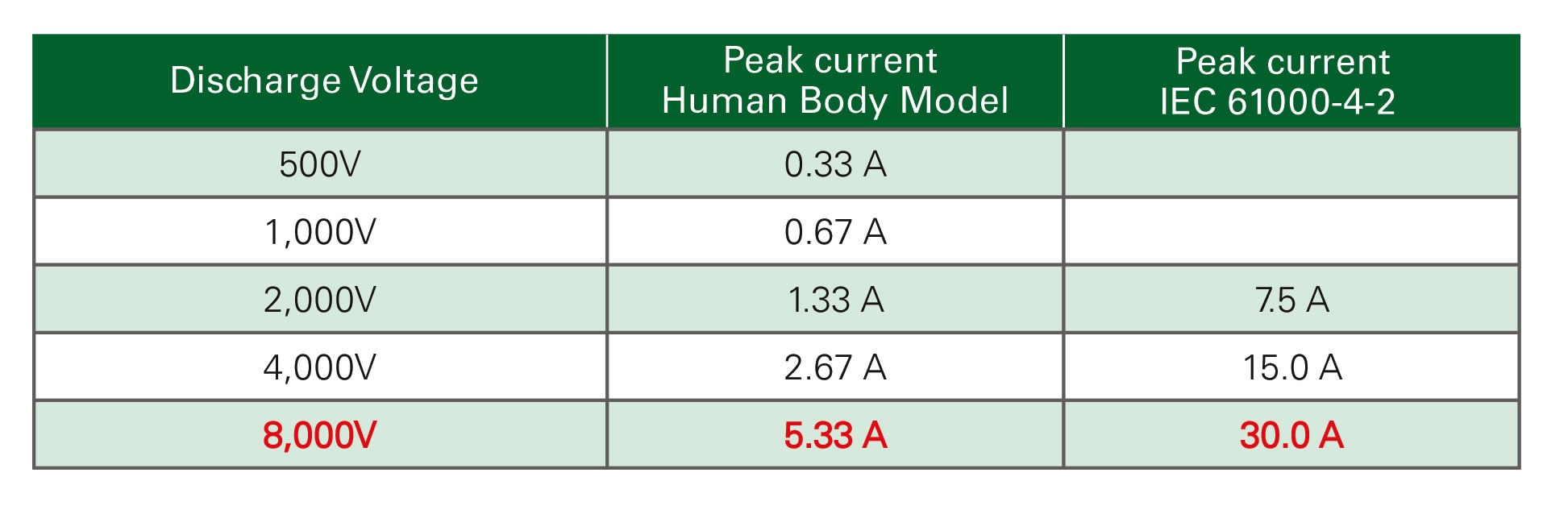
Table 2: ESD events outlined
Products that are directly connected to the AC mains (120V to 250V AC rms) may be exposed to severe surge transients (lightning, load switching, etc.) and short circuit/overload conditions, making it necessary to fit a combination of components to protect against overcurrent (fuses or PTCs) and overvoltage (MOVs, TVSs, or TVS diode arrays). Standards that may specifically require this protection are:
- IE 61000-4-4 (EFT user level environment)
- IEC 61000-4-5 (lightning induced surges)
- IEC/EN 60950-1 (safety standard)
Portable consumer products that contain an AC or DC adapter may have specific ESD and low-level lightning exposure threats that must be considered. Standards that may specifically require this protection include:
- IEC 61000-4-2 (ESD user level environment)
- IEC 61000-4-5 (lightning induced surges)
Keypads or other manual interface buttons may be an entry point for the destructive energy of ESD. Audio lines may have similar ESD exposure due to the speaker wire connections and exposure to manual handling. Connectors for S-Video, composite video and HDMI are also susceptible to ESD exposure since they often undergo manual handling. Battery pack applications will endure similar ESD exposure as well as potential overcurrent run-away conditions that must be protected against (IEC 61960 & IEC 62133 specifically apply). Low-speed and high-speed data lines, too, have an ESD exposure; depending on their actual placement, they may also be exposed to lightning-induced surge events. International standards that typically apply for these types of applications include:
- IEC 61000-4-2 (ESD user level environment)
- IEC 61000-4-5 (lightning induced surges)
Consumer products face an ever increasing risk of being damaged by overvoltage transients such as ESD. As IC designers continue to pack more functionality into their chipsets, there has been a major decrease in built-in ESD survivability — which makes it necessary to employ external protection components. Equipment manufacturers test their equipment to the international IEC 61000-4-2 standard; to ensure the life expectancy of their products, TVS diode arrays are recommended for protection. TVS diode arrays are not only able to meet ICs’ small footprint requirements, they can also offer very low clamping voltages compared to competing technologies, which means they are capable of safeguarding state-of-the-art ICs. Exposure to EFTs, nearby lightning strikes, or potential power fault events in turn make it essential to put overcurrent and overvoltage protection solutions in place. By employing the correct overcurrent and overvoltage protection components, manufacturers can ensure their products remain an integral part of their consumer’s life. Choosing the right protection components also ensures that applications comply with regulations relating to both safety and functional factors.
About the authors
Phillip Havens is a Principal Engineer at Littelfuse and holds a BSEE and MSEE from Louisiana Tech University. He represents Littelfuse at electronics safety, circuit protection, and telecom-related industry associations such as ITU, TIA, ATIS, IEC, IEEE, PEG, and UL497/60950-1/62368-1 STPs. He also helps define, direct, and support the company’s silicon-based protection product lines.
Chad Marak is Director of Technical Marketing and TVS Diode Array Products in the Semiconductor Business Unit of Littelfuse, Inc. He received his BSEE from Texas A&M University and MSEE from Santa Clara University. He has been in the semiconductor industry for 10 years and holds four US patents.
Product Spotlight
APV1111GVY
Panasonic

Panasonic PhotoMOS® Photovoltaic MOSFET High-Power Drivers
| SKU: | |
|---|---|
| Stock: | 3490 |
| Cost: | $3.95 |
