ON Semiconductor Expands ESD Protection Technology into Industry’s Smallest Package for Use in Portable Electronics Applications
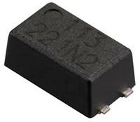
ON Semiconductor has introduced two ESD protection devices housed in its new, ultra-small 0201 Dual Silicon No-Lead (DSN-2) package. The DSN style package, which measures a mere 0.6 mm x 0.3 mm x 0.3 mm, enables 100 percent utilization of the package area for active silicon, offering a significant performance-per-board-area advantage compared with products in plastic molded packages.
The company’s first offerings in the new package are the ESD11N5.0ST5G and ESD11B5.0ST5G which are an expansion of its high performance off-chip ESD protection portfolio. By expanding its ESD protection portfolio into the industry’s smallest package, ON Semiconductor can offer devices that are ideal for safeguarding data lines in portable applications where board space is often extremely limited such as cell phones, MP3 players, PDAs, and digital cameras.
The ESD11N and ESD11B are the next generation of proprietary ESD protection technology from ON Semiconductor which boasts best in class clamping voltage. With the combination of the industry’s lowest clamping voltage and smallest package, ON Semiconductor is providing an unparalleled ESD protection option. The reduced size and bidirectional single line designs provide ultimate flexibility and ease of routing to fit the products into a variety of space constrained applications. The new 0201 DSN-2 package measuring a mere 0.6 mm x 0.3 mm x 0.3mm provides a 3X board space saving compared to the popular SOD-923 (also known as 0402) package.
The ESD11N is a 0.6 pico farad (pF) device that utilizes patented integrated ESD technology from ON Semiconductor which enhances clamping performance while maintaining low capacitance. The low capacitance value ensures that this device has negligible impact on the signal integrity of high speed data lines making it ideal for applications such as USB2.0 and HDMI. In addition, the ESD11N maintains less than 0.5 decibel (dB) insertion loss up to 3 gigahertz (GHz) and excellent capacitance linearity over voltage and frequency making it suitable for protecting high frequency antenna lines with minimal effects. The ESD11B is a 15 pF device that expands ON Semiconductor low clamping ESD protection technology into the new 0201 DSN-2 package to provide a protection option for general purpose and low speed data lines that have tight board designs with limited room.
Both new ESD products clamp an input ESD waveform of 8 kilovolts (kV) per the IEC61000-4-2 contact standard, to less than 10 volts (V) in a matter of nanoseconds. This clamping voltage performance leads the industry and ensures protection for the most sensitive integrated circuits.
“As our customers are continually challenged to improve the ESD protection on ever shrinking designs, ON Semiconductor has responded with new innovative protection devices in the space saving 0201 DSN-2 package,” said Gary Straker, general manager and director of ON Semiconductor’s Protection and Control division. “Incorporating ON Semiconductor’s leading protection technology into this breakthrough package design is a prime example of the company’s focus on developing targeted solutions to the industry’s growing protection needs.”


