
Integrated passives & protection devices make a good match
There can be little debate about the benefits of the miniaturisation of electronics devices and their ever-increasing functions, but they can give designers headaches; when marketing departments freeze the form factor and specifications of the end-device, designers and PCB layout experts must deal with it, making their jobs a balancing act. Once the core ICs have been selected and placed on the board, they must design basic, but essential, circuits for impedance matching, ESD protection, line termination and filtering.
Traditionally achieved with discrete devices, new integrated solutions offer significant space savings compared to standard-size components like 0402, 0201 or even 01005 SMD. The right trade-off between flexibility and overall space savings is critical. Benefiting from their accrued in-depth application knowledge, semiconductor companies have developed products for many design cases that don’t compromise performance or board space.
This space saving, won by integrating discrete components into a single chip, is the result of three factors. First, when integrating separate components on a die, semiconductor engineers can use a single bandgap to cover the complete die. Second, mounting a component on a PCB leaves a gap - called pitch - between nearby packages to evacuate solder excess, avoiding the ‘tombstoning’ phenomenon or other common assembly defects. Third, interconnecting discrete components on a board devours millimetres of metal lines and space-consuming vias, while semiconductor engineers can interconnect the discrete components on silicon die with micrometres of metal lines. These tiny interconnections created by the semiconductor process contribute to decreasing the overall space needed and drastically reduce the undesired parasitic effects of the metal lines (parasitic resistor, inductor and capacitor). Designers working on EMI rejection know a low-parasitic solution is crucial to avoiding multiple design and layout iterations and matching the specified pattern.
Integrating passive and active components in a single package additionally benefits the tolerance range due to semiconductor process control. Matching components processed on the same die from the same wafer is far easier than matching discrete components manufactured separately. For instance, ESD protection on differential high-speed lines (HDMI, USB 3.0...) matching the capacitance of the differential lines is far easier to achieve when using dual-line ESD protection (single package) than two single-line ESD protection devices (two separate packages from different lots). The use of integrated passive and active devices simplifies simulations and reduces the parameters involved in corner-lot analysis. By replacing discrete components with an off-the-shelf solution, designers accelerate time-to-market with an improved form factor and better performance.
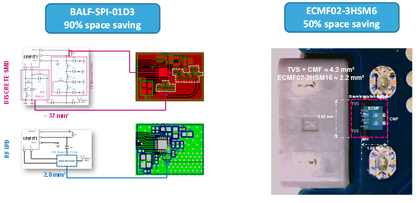
As an example, STMicroelectronics’ ECMF02-3HSM6 (Common-Mode Filter embedding ESD protection) or BAL-SPI-01D3 (outsmarting ultra-miniature balun, which integrates matching network and harmonics filter) enables 50% to 80% space saving on the PCB and perfectly matches integrated components. Liberating the constraints on PCB size, these devices speed up time-to-market and reduce both BOM count and the cost of assembly.
Product Spotlight
APV1111GVY
Panasonic

Panasonic PhotoMOS® Photovoltaic MOSFET High-Power Drivers
| SKU: | |
|---|---|
| Stock: | 3490 |
| Cost: | $3.95 |
