
A test method for synchronising multiple GSPS converters
By Shane Foss & Rob Reeder, Analog Devices.
Overview and methods
Synchronising multiple ADCs is an essential requirement in the aerospace and defence industry. Synchronisation is defined as the ability to match each converter to an accuracy equal to or less than a single clock cycle dependent only upon the aperture jitter of the ADC, clock jitter and clock distribution accuracy. The AD9625, a 12-bit, 2.5GS/s ADC, was designed to facilitate this synchronisation and utilises high speed serial data lanes conforming to the standard JESD204B interface technology. JESD204B based converters are still relatively new in the market and there is concern over the ability to synchronise multiple devices. This paper should reduce some of these concerns by showing that a relatively simple bench test was used to successfully synchronise two converters and show scalability.
There are two options for synchronising multiple AD9625’s together. Although both methods are features of JESD204B sub class 1, the ‘time-stamping’ method will be the focus of this article, primarily because there is no need to measure the time delay from every converter to every FPGA and because with deterministic latency, latency would have to be adjusted for each individual data path in order to correct the timing mismatch.
One key application that will benefit from synchronisation is RADAR. In this case, the designer only needs to think about the relative time from one receiving element to the next. In addition, the data processing is less intensive when using time-stamping because the FPGA or processor is only looking for a time marker in each data set. Using this time marker allows the designer to align the data and run algorithms from a defined and synchronous point for each converter path. There are no concerns about the distance in trace length from each converter to its respective FPGA. This routing is even likely cross over multiple boards making it all the more helpful in the application design. This paper gives guidance on basic design rules to follow when synchronising high-speed GS/s converters.
A note about JESD204B
The AD9625 is a 12-bit, 2.5GS/s high-speed ADC with serial outputs that follow the JESD204B standard. Within the JESD204B standard there are multiple subclasses which are optimised for varying purposes.
The AD9625 uses subclass 1 which is critical to how this method of synchronisation is performed. Subclass 1 uses a SYSREF signal for aligning the serial output data. The SYSREF signal essentially gets clocked into the output data of the converter, where it can synchronise to the conversion clock and ensure that each distributed SYSREF signal arrives at each converter simultaneously. This generates a marker or time stamp for the JESD204B serial output data showing the exact point where the synchronised data analysis should start.
The AD9625 provides two options for using this marker where the designer can use a separate control bit which is part of the entire 16-bit JESD word or replace the LSB of the converter with the SYSREF time-stamp; the test described in this paper used the LSB option.
The test setup
The setup in Figure 1 shows how to synchronise two converters. In theory, however, there is no limit to the number of converters that can be synchronised. Starting with a properly designed AD9625 board, the test setup requires the following equipment:
- (2) standard desktop/laptop computers running Windows;
- (2) Xilinx VC707 development kits;
- (2) AD9625 FMC board, PN: AD-FMCADC2-EBZ;
- (1) Tektronix HFS 9009, pulse generator and stimulus system;
- (2) Rohde & Schwarz SMA 100 A signal generator w/ option B22, low phase noise option; and
- (2) 24GHz matched RF cables for the clock and SYSREF connections.
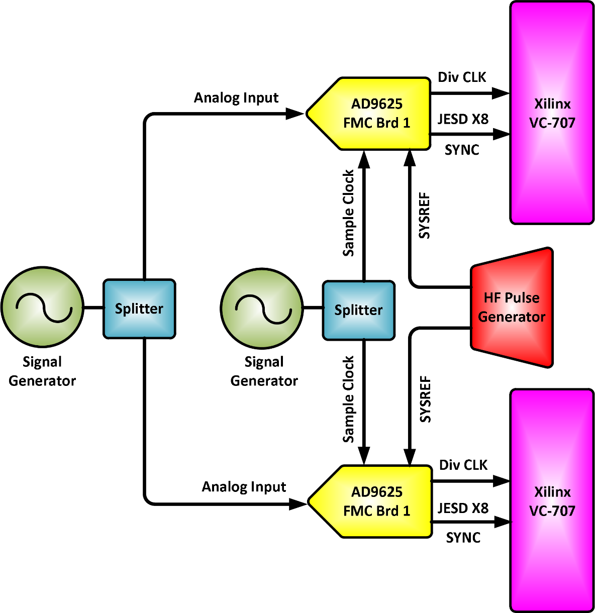
Figure 1 - a block diagram of the test setup and its major interconnects
The signal generator (SMA 100 A) provides the 2.5GHz sampling clock for each converter. A single output was then split into two clocks by using a 5350-244 Picosecond Pulse Labs power divider. From the two divided outputs a pair of phase and length matched cables are connected to each AD9625 board, ensuring that the clock will be synchronous when arriving at each converter.
The pulse generator (HFS 9009), was specifically chosen to generate the SYSREF signals because it provided multiple differential outputs with reasonably low jitter and the ability to skew one differential output relative to another allowing for the ability to move the placement of the SYSREF signal relative to the sampling clock.
Next the analogue input must also be split in the same way as the sample clock, using another power divider with a pair of phased matched cables to ensure both analogue input signals arrive at each converter’s input at the same in time.
The AD9625 (AD-FMCADC2-EBZ) board connects to the VC707 evaluation platform via an HPC FMC connector. The Xilinx Chipscope and SDK software tools were used to interface with the VC707 and implement the time-stamping procedure and capture the data.
The test procedure
To manually trigger SYSREF, the pulse generator is activated to align the SYSREF signals for each converter. Upon detection of a SYSREF marker each FPGA will perform a data capture.
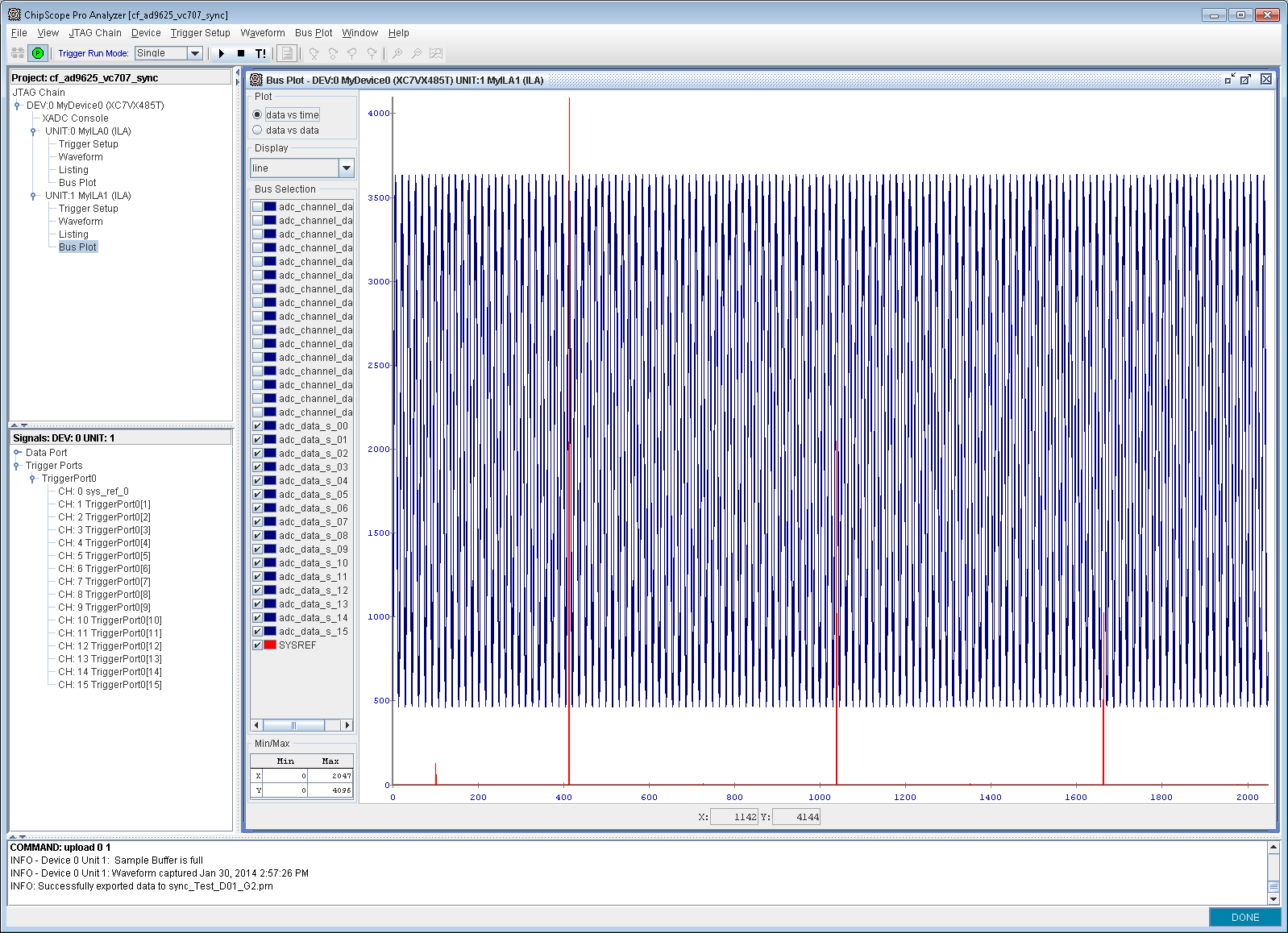
Figure 2 - Xilinx Chipscope screen capture displaying a triggered data capture with SYSREF
Each red line represents an LSB SYSREF marker while the blue waveform shows the actual captured data. Once the data is successfully captured, as shown above in Figure 2, the data is exported to Matlab.
Synchronised results
After analysing the exported raw data into Matlab, the time domain reconstructed data from each ADC can be plotted on top of each other, Figure 3 below.
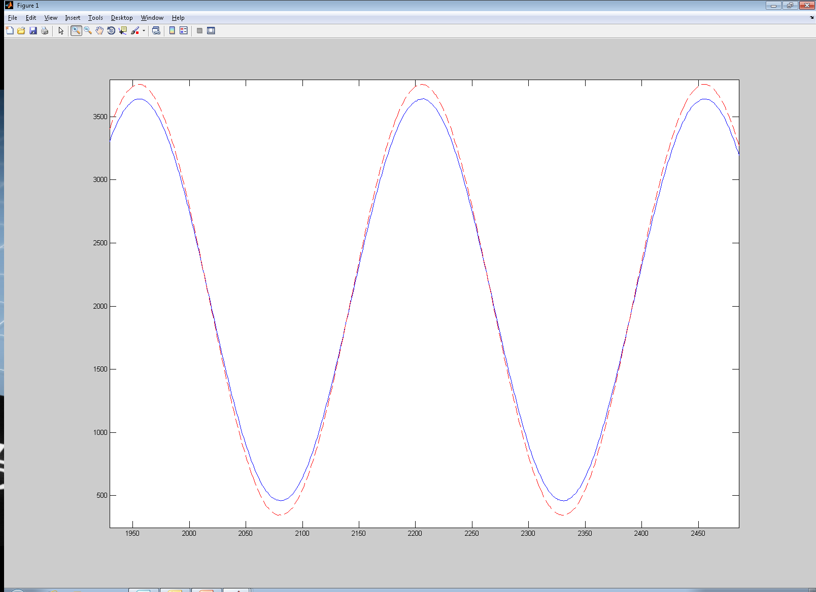
Figure 3 - Matlab reconstruction of raw data in the time domain
Figure 3 shows the rising edge of the reconstructed time domain data. The horizontal axis represents samples. The delta between the blue and red lines representing the two separate and synchronised ADC/FPGA captures, and visually this looks to be well less than one sample deviation.
Table 1 below, reviews a subset of the sample phase deltas as it relates to the test configuration setup in Figure 1 with a 710MHz analogue input.
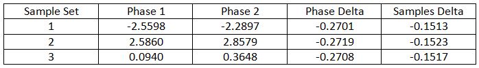
Table 1 - subset of sample phase deltas
The test results above show an analogue input running at 710MHz and three separate captures yielded similarly accurate results. Again each result is synchronised to within ±0.5 samples. Note it is very important to phase lock the two sources in the test setup to provide synchronous sample clock and SYSREF inputs. Without phase locking then statistically the expectation would eventually violate the setup and hold times every so often.
With new and upcoming JESD204 clock distribution ICs on the market, like the HMC7044, AD9525 and AD9528 this will automatically take care of phase locking of each clock and SYSREF input.
Conclusion
Using this test setup method proved that two AD9625, 12-bit, 2.5GS/s ADCs can be synchronised with a JESD204B high-speed serial digital interface to better than one sample accuracy using the SYSREF and time-stamping method. While this method used plenty of bench top testing equipment, which is cumbersome, it will soon be possible to implement this same synchronisation setup using newly released Analog Devices Inc. clocking devices allowing for a simpler solution.
In addition to proving synchronisation between two converters, this paper has also outlined that this concept can be scaled to incorporate multiple converters, where applications such as RADAR, electronic warfare and military communication applications would benefit greatly from this new capability at GS/s speeds.
Product Spotlight
APV1111GVY
Panasonic

Panasonic PhotoMOS® Photovoltaic MOSFET High-Power Drivers
| SKU: | |
|---|---|
| Stock: | 3490 |
| Cost: | $3.95 |
