
A look at the latest developments in non-volatile memory
The rate at which modern devices generate data means it should come as no surprise that manufacturers are still actively developing alternative and - hopefully - improved non-volatile memory solutions. Philip Ling, Editor, ES Design magazine, takes a look at some of the most recent developments.
If embedded control design can be categorised as comprising three key elements, they would probably be digital processing, mixed-signal interfaces, and memory. Of the three memory has, perhaps, seen the least amount of active development over recent years, but that may be changing. The promise of a truly unified memory for embedded applications may still be elusive, but there is now a range of technologies that provide non-volatility in devices that, traditionally, would have had to make do with volatile (RAM) in order to meet performance and density requirements.
Standard Flash memory in both discrete devices and integrated alongside microcontrollers has become the ‘default’ solution to long-term and non-volatile storage, but thanks to some innovative thinking Flash-like solutions are emerging that could provide the next step towards a unified memory. Cypress uses its SONOS (Silicon-Oxide-Nitride-Oxide-Silicon) process to create a non-volatile form of SRAM that it uses in both discrete and integrated devices. The process uses Fowler-Nordheim Tunnelling to store data in a nitride layer (Figure 1), in a cell that is integrated alongside a standard SRAM cell (the process only requires two additional masks), which results in devices that have a one-to-one ration between SRAM cells and non-volatile cells. In the event of a fault (such as loss of power), the entire contents of the SRAM cells are transferred to the non-volatile cells.
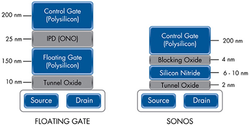
Figure 1 - Cypress employs its SONOS technology for its nvSRAM devices
Cypress has just announced a family of 16Mb nvSRAM, which includes the first nvSRAMs to integrate the Open NAND Flash Interface (ONFI) Standard 1.0 interface, supporting direct connection to NAND bus controllers. Devices with an optional real-time clock feature allow time-stamping of critical data, and the SONOS technology offers 20-year data retention.
Split gate
While Cypress’ SONOS-based nvSRAM is a NAND Flash technology, there are also developments in the world of NOR Flash, too. Microchip has recently introduced a 64Mb NOR Flash device, arranged as 4M x 16, based on the SuperFlash technology developed by Solid State Technology (now a Microchip company). As Figure 2 shows, it uses a split-gate architecture, which is said to deliver more reliability than other non-volatile solutions. The thick-oxide process is also claimed to require fewer mask steps, resulting in a lower cost per bit. The nature of NOR Flash means random access read times are around 70ns for the 64Mb device, while page read access times are 25ns. Sector and block erase times are also a feature; 18ms, while the entire device can be erased in 40ms. Its 100,000 endurance cycles and more than 100 years data retention are also relevant figures of merit.
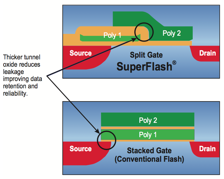
Figure 2 - Microchip's non-volatile technology
Another promising non-volatile memory technology that also promises improvements over conventional Flash memory is Resistive RAM. Last year, Panasonic announced it was introducing an 8-bit MCU that integrates 64kB of ReRAM, which Mouser is now stocking. In this application, the majority of the ReRAM is used as a Flash replacement, while 2kB intended to be used as EEPROM. The technology is often compared favourably with phase-change and magneto-resistive RAM, as it’s faster and simpler respectively. Of all the potential technologies to emerge as the solution to ‘unified’ memory, ReRAM is probably the slowest to be adopted; Panasonic has chosen to integrate alongside a simple MCU rather than develop a standalone product family (at least, to date), which may indicate it has some commercial and/or technical issues with respect to supplanting standard Flash in every application space.
However, in this implementation, Panasonic states it has reduced the overall power by 50% when compared against the previous generation of the MCU, which employed conventional Flash memory. Another benefit of ReRAM is it doesn’t require a separate erase cycle, while having write cycles that are five times faster than Flash or EEPROM. The memory cell structure stores bits based on the resistance of a thin metal-oxide film, sandwiched between two electrodes. The cell represents a logic-1 by a low resistance, which is achieved by applying a pulsed negative voltage to the top electrode. This causes oxygen ions to migrate in to the tantalum oxide, lowering the resistance and making the cell more conductive. By applying a positive pulse to the top electrode, oxygen ions migrate away from the tantalum oxide, thereby raising the resistance. This simple structure of metal oxide stacked vertically between two electrodes delivers both low power consumption and high speed rewriting.
Unified memory has long been pursued within the industry, with many alternative technologies in development. Given the level of dependence on non-volatile data storage today, it seems reasonable to expect the research to continue.
Product Spotlight
APV1111GVY
Panasonic

Panasonic PhotoMOS® Photovoltaic MOSFET High-Power Drivers
| SKU: | |
|---|---|
| Stock: | 3490 |
| Cost: | $3.95 |
