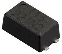
Low-jitter clock is designed for high-data rate requirements
Analog Devices has introduced the AD9528 JESD204B clock and SYSREF generator, defined to support the clock requirements for long-term evolution and multicarrier GSM base station designs, defence electronics systems, RF test instrumentation, and other emerging wideband RF GSPS data acquisition signal chains.
The use of the JESD204B standard for the high-speed converter-to-digital processer interface is becoming increasingly prevalent across many state-of-the-art applications, as data rates are being pushed into the multi-Gb/s range. Additionally, multi-channel synchronisation and data latency management are becoming a system necessity. The JESD204B interface was specifically developed to address high-data-rate system design needs, and the AD9528 clock device contains functions that support and enhance the unique capabilities of that interface standard.
The AD9528 provides a low-power, multi-output, clock distribution function with low-jitter performance, along with an on-chip, two-stage PLL and VCO. The on-chip VCO tunes from 3.6 to 4.0GHz, with the input receivers and oscillator providing both single-ended and differential operation.
The AD9528 provides JESD204B-compatible subclass 1 SYSREF and deterministic latency clocking signals, and supports a variety of options for SYSREF signal generation. The most basic is a simple buffer function wherein the user-provided SYSREF signal is fanned out to the SYSREF output pins. When provided with an external SYSREF source, the AD9528 is able to synchronise the SYSREF outputs to the clock outputs being generated internally, which is necessary to achieve accurate deterministic latency.
The AD9528 is also capable of generating the SYSREF source internally. As well as continuous signal SYSREF generation, the AD9528 supports ‘n-shot’ pulse generation. N-shot generation is vital in systems where a continuous signal might result in unwanted spurs in the output spectrum of the data converter being clocked.
When connected to a recovered system reference clock and a VCXO, the AD9528 generates 12 low-noise outputs ranging between 1 and 400MHz, and two high-speed outputs at up to 1.25GHz. The frequency and phase of one clock output relative to another clock output can be varied by means of a divider phase-select function that serves as a jitter-free, coarse timing adjustment in increments that are equal to half the period of the signal coming from the VCO output. The SYSREF signals each have additional phase offset capability, making it easy to dial-in the optimal arrival time at each target device.
The AD9528 can be designed into wideband RF data acquisition applications with ADI’s AD9680 dual-channel, 14-bit, 1.0-GSPS JESD204B A/D converter.


