
Newer nodes enhance FPGA performance
Sally Ward-Foxton investigates how more advanced process nodes are enabling performance enhancements in the latest-gen FPGA products.
Today’s semiconductor foundries are continuously battling to be the first to achieve smaller process nodes, even with the physical limits of some of the process technologies beginning to appear. For FPGA makers, who depend on using advanced nodes as a way to differentiate their product offerings, moving to the next node usually enables a whole new generation of products. What benefits do these newer nodes offer to FPGA users, and do the benefits outweigh the limitations?
Upgrading to use the latest process technologies can mean significant performance advantages, explains Giles Peckham, Regional Marketing Director, Americas & EMEA at Xilinx. Xilinx is currently delivering 20nm devices in its Kintex UltraScale and Virtex UltraScale FPGA families, including both monolithic and 2nd gen 3D-IC devices. A combination of the company’s UltraScale architecture and the 20nm process node provides ASIC-class system-level performance for very high-end applications.
“Customers may choose to migrate their designs from our 7-series 28nm all-programmable FPGA families for a number of reasons, including performance, integration, cost or power,” says Peckham. “For example, some high performance designs may be migrated from Kintex-7 to Kintex UltraScale to achieve more than one speed-grade advantage in logic performance, nearly three times higher DSP bandwidth, 2.6 times higher transceiver bandwidth and DDR4 interface speeds of 2400Mb/s,” he says. “Other designs may be migrated from Virtex-7 to Kintex UltraScale, achieving the same or in some cases higher performance at much lower cost and 25 to 45% lower power.”
“Alternatively, Virtex-7 designs may be migrated to Virtex UltraScale to benefit from more than a one speed-grade advantage in logic performance, more than double the total transceiver bandwidth and DDR4 interface speeds of 2400Mb/s,” he adds.
However, Peckham points out that although the newest process nodes offer advantages to high-end applications, not all designs will benefit from migrating from 28 to 20nm. “Although Moore’s Law has not run out of steam, and integration, performance and power consumption all continue to improve, the manufacturing cost per gate is no longer reducing with each new process node,” he says. “For many smaller and lower performance designs, the 28nm node is still the most cost effective.”
Xilinx uses TSMC’s 20nm process technology, which TSMC claims can provide 30% higher speed, 1.9 times the density, or 25% less power than its 28nm technology. This process uses the same planar transistor architecture as older nodes, scaled down, which hasn’t been without its difficulties. The physical limits of using 193nm-wavelength lasers to etch the wafers were reached at 28nm feature size, so for 20nm, TSMC is using a technique called double patterning. This involves using two photo-masks, each with half the pattern, one after the other, to increase the resolution of the features that can be produced. Unfortunately, this technique adds complexity and several steps to the process, increasing the cost. There may be a bright side, though. Depending on the device and the application, cost benefits may become apparent when looked at from the system level, despite the apparent increase in cost-per-transistor.
“Integrating multiple devices from a previous node into one new device, achieving the same performance with fewer pins or achieving lower power for the same design might all lead to system-level cost reductions, so the total cost of ownership calculation is becoming more complex,” says Peckham. “Xilinx now employs a multi-node strategy, supporting the most appropriate solution for each design, regardless of process node.”
Migrating to FinFET
Another FPGA-maker taking advantage of the latest process technologies is Altera. The company has adopted Intel’s 14nm process for its next-gen devices, which according to the company, puts FPGAs a step ahead of competing device types.
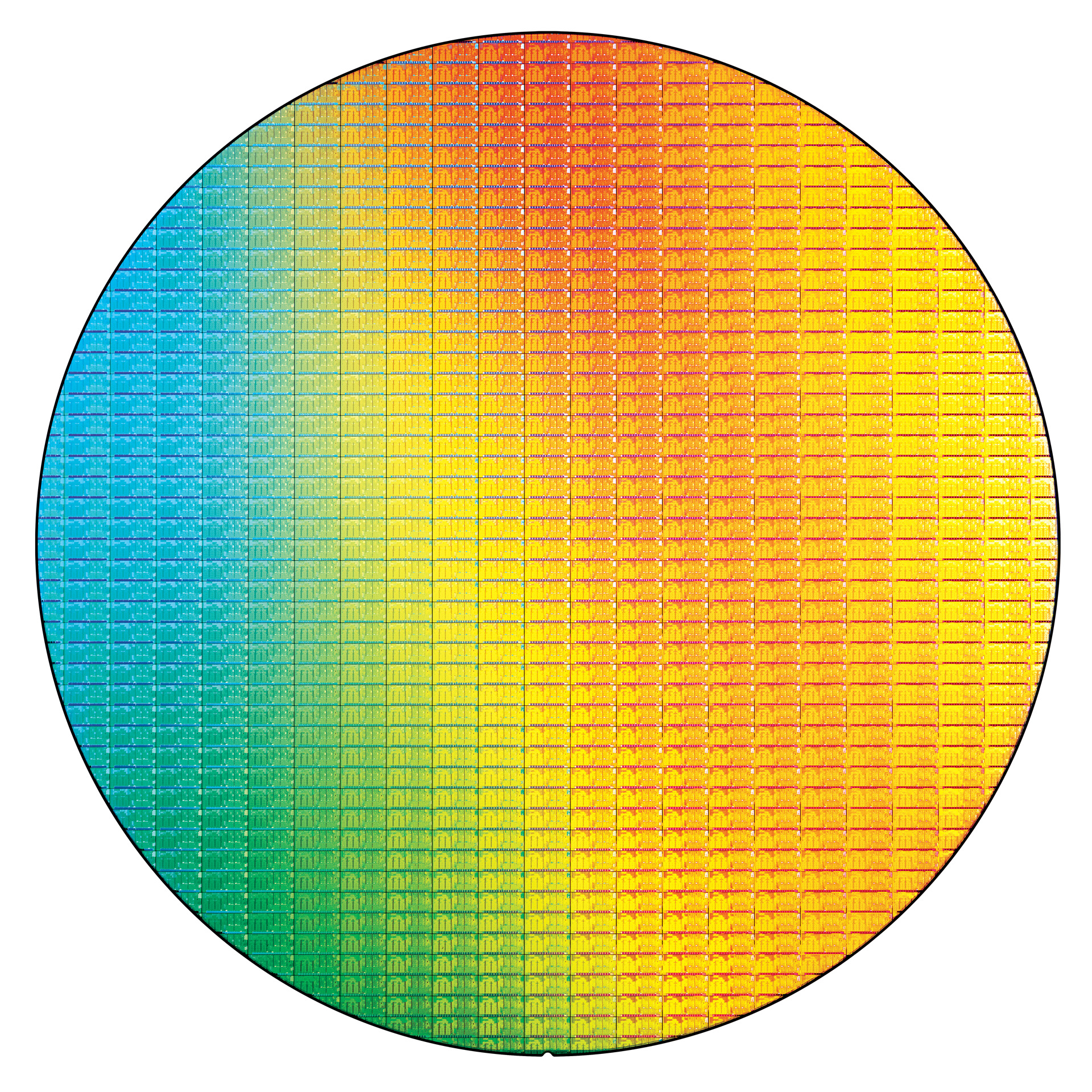
Figure 1 - An Intel 14nm wafer, codenamed ‘Broadwell’, uses the finFET transistor architecture for improved performance
“One of the biggest advantages that FPGAs offer over competing ASICs and ASSPs is an FPGA’s ability to scale to the most advanced process nodes,” says Jordon Inkeles, Senior Marketing Manager for high-end FPGAs at Altera. “The combination of Intel’s 14nm TriGate process and Altera’s high-performance HyperFlex architecture allow Stratix 10 FPGAs and SoCs to deliver two times higher core performance compared to the previous generation of high-end FPGAs.”
How did Altera make the decision to move to the next process node - aren’t there risks associated with moving to brand new process technologies? “There are always considerations we must make as a company when we choose to migrate to the next process node - specifically power, performance and cost considerations,” Inkeles says. “14nm is Intel’s 2nd gen working with Tri-Gate technology, following Intel’s highly successful 22nm Tri-Gate deployment, with over 100m units shipped by Intel since going in to production. This demonstrates maturity and a low risk path to production using this advanced technology.”
Intel’s aim with its 14nm TriGate process is to reduce the thickness of its processor cores to 7.2mm, down from 26mm in 2010, and to enable low-power fanless designs for devices such as tablets. “Intel’s 14nm technology is now qualified and is in volume production,” says Mark Bohr, Intel’s Senior Fellow. “This technology uses a 2nd gen of TriGate, or FinFET, transistors that provide industry-leading performance, power, density and cost per transistor.”
FinFET is largely thought of as the biggest shift in semiconductor technology in more than 40 years. First conceived in the 1990s, it was thought that a multi-gate structure would reduce leakage current. FinFETs today are 3D structures, increasing the volume of the gate compared to a 2D planar structure for the same unit area. Since the Gate wraps around the conducting channel it can control it very closely, so that very little current is allowed to leak when in the off state. Lower threshold voltages can be used, leading to lower power consumption. The Source and Drain are implemented as thin ‘fins’ either side of the conducting channel.
Intel began using the FinFET architecture in its 22nm process technology, but the newest process node to be announced, 14nm, reduces the key dimensions of the transistors’ features. Transistor fin pitch was reduced from 60 to 42nm, transistor gate pitch was reduced from 90 to 70nm and the interconnect pitch was reduced from 80 to 52nm (Figure 2). “These three process features combined add up to a true 14nm technology with good dimensional scaling,” Bohr says. “Fin pitch is reduced from 60 to 42nm so now they are packed more closely together for improved layout density,” says Bohr. “In addition, we have made the fins taller and skinnier. That helps to improve the performance or the drive current of these transistors. Because we are getting more drive current per fin, or more performance per fin, we can design circuits using fewer fins, so we have depopulated some of the fins,” Bohr adds. “This gives us even better density scaling and some capacitance reduction, and of course, capacitance reduction translates to lower active power.”
 compared with microscope pictures of the actual devices (bottom).jpg)
Figure 2 - Schematic of the changes to Intel’s finFET design for the new 14nm process node (top) compared with microscope pictures of the actual devices (bottom)
Altera says that the densities delivered by the new process node enable it to provide in a single monolithic die what other companies are currently achieving with multi-die 2.5D devices. “Only the Intel 14nm Tri-Gate process offers a die shrink over the 20nm process node,” Altera’s Inkeles says. “Other foundries who will offer competing FinFET based process technologies with 14 or 16nm FinFET transistors are using 20nm backend design rules which limits the die shrink they get, compared to the 20nm node, thereby providing Altera with performance, power, density and cost advantages.” Stratix 10, which is the first Altera device to be produced on 14nm, remains on schedule for tapeout in early 2015 and shipping silicon later in the same year, according to Inkeles.
Product Spotlight
APV1111GVY
Panasonic

Panasonic PhotoMOS® Photovoltaic MOSFET High-Power Drivers
| SKU: | |
|---|---|
| Stock: | 3490 |
| Cost: | $3.95 |
