
Evaluating SERDES in FPGAs
Supporting multiple high-speed transmission interface standards and accelerating time-to-market with economical SERDES enhanced FPGAs. By Benny Ma, Applications Engineer, Lattice Semiconductor.
The convergence of FPGA and high-speed SERDES technologies has led to the emergence of SERDES-enhanced FPGAs as a cost-effective alternative to ASICs in applications which require a multi-Gigabit data link across a PCB, backplane or cable. This new class of programmable devices is changing the way many products are designed, particularly as these devices are becoming available at increasingly lower-power and lower-cost.
Originally developed for high-performance packet processing and routing elements in carrier-class networking equipment, FPGAs equipped with embedded SERDES transceivers have been available for over a decade. Combining low-power multi-Gigabit SERDES transceiver cores with a price-optimised FPGA architecture creates a versatile solution platform for applications which make extensive use of SERDES-based interfaces such as Ethernet (XAUI, GbE, SGMII), PCIe (PCI Express) SRIO (Serial RapidIO) and Common Public Radio Interface (CPRI). These include small-cell wireless infrastructure, microservers, broadband access, industrial video and other high-volume applications where low cost, low-power and small form-factors are key design constraints.
Many of the early applications to embrace SERDES-enhanced FPGAs have been innovative RF, baseband and backhaul products which address the needs of wireless network operators. Virtually every carrier throughout the world is making massive investments to upgrade their infrastructure as they struggle to keep pace with the explosive growth in demand for mobile data and video traffic. In addition to upgrading their existing base stations to support high-capacity 3GPP/4G wireless standards, many operators are embracing a new Heterogeneous Network (HetNet) architecture in which the traditional macro infrastructure is supplemented by a new class of Low Power Nodes (LPNs) such as small cells, low power remote radio heads, and relays (Figure 1).
 combine zero footprint versions of traditional macro architecture with a variety of new low power, low cost network elements..PNG)
Figure 1 – Today’s evolving wireless Heterogeneous Networks (HetNets) combine zero footprint versions of traditional macro architecture with a variety of new low power, low cost network elements.
These compact, low-power (typically between 100mW and 10W) wireless nodes can add capacity in high-traffic areas or extend wireless coverage into buildings, public spaces, and urban canyons which are beyond the reach of conventional base stations. This requires LPNs to be highly configurable in order to support multiple air interface standards and RF frequencies, compact and rugged enough to blend into the urban landscape, and inexpensive enough to justify widespread deployment.
In any LPN, FPGAs with SERDES capabilities can be used to implement data path bridging and interfacing and the packet-based network interfaces (GbE, 10GbE/XAUI, XGMII) commonly used to connect small-cell clusters with the backhaul infrastructure. They can also be used to implement the XGMII interface and most of the digital functionality in smart SFP (small form-factor pluggable) transceiver products, commonly used in broadband access equipment.
Like most SERDES-Enhanced FPGAs on the market today, Lattice Semiconductor’s ECP5 FPGA family uses embedded SERDES transceivers which provide the baseline functionality required to support most commonly-used high-speed serial interfaces. The ECP5 series includes devices with varying amounts of programmable logic elements (up to 85,000 LUTs) and up to four transceivers. The transceivers are implemented as pairs within a Dual Channel Unit (DCU) containing a single shared reference clock input and Tx PLL. Each SERDES channel can be configured independently to perform high-speed, full-duplex serial data transfers at data rates from 270Mb/s to 3.2Gb/s (Figure 2).
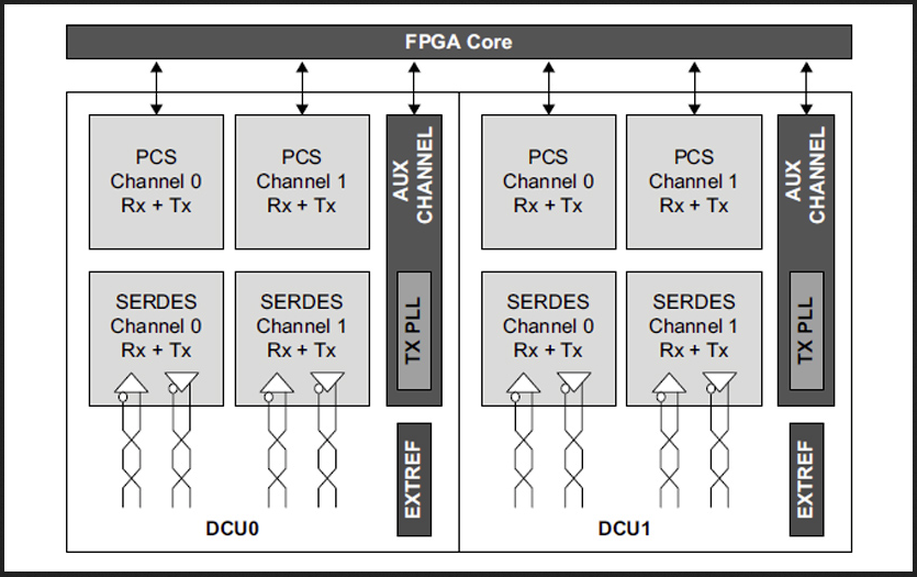
Figure 2 - Block diagram of the dual-channel SERDES element used in the ECP5 FPGA series.
Data coding
The Physical Coding Sublayer (PCS) logic in each channel can be configured to support several types of Ethernet interfaces and several other common networking and system interconnect standards. Since transceiver power consumption varies according to how its configured and which features are used, no single number could be considered accurate. But, as a first-order approximation, its safe to say that in most simple configurations, a single channel 3.25Gb/s SERDES consumes less than 0.25W. Quad-channel SERDES elements which support similar functions often consume under 0.5W. Different combinations of protocols within a DCU are permitted subject to certain conditions as specified in the ECP5 SERDES Usage Guide.
Soft IP can be used in conjunction with the SERDES channels to support protocol level function for high-speed serial data links such as PCIe, CPRI, SD-SDI, HD-SDI and 3G-SDI. For custom applications, the user can use his own protocol level logic, giving users full flexibility to design their own high-speed data interface. The PCS also provides bypass modes that allow a direct 8- or 10-bit interface from the SERDES to the FPGA logic, allowing user to implement their own data coding.
In order to compensate for the Inter-Symbol Interference (ISI), attenuation, reflection, and other phenomena which SERDES signals encounter as they traverse printed circuit boards or cables, the transceiver uses a combination of transmitter and receiver equalisation techniques which can be programmed via the device’s configuration registers. The transmitter’s high speed line driver has adjustable amplitude settings and termination resistance values which can be optimised for attenuation due to the length of the channel, and adjusting termination resistance to match the channel trace impedance to minimise signal reflection. It can also perform transmit equalisation using adjustable pre/post-cursor de-emphasis settings which reduces inter-symbol interference (ISI) caused by interactions between the bit being transmitted and the energy from the previously-transmitted bit still present in the transmission line.
The receiver includes a Linear EQualiser (LEQ) which is used to selectively amplify the frequency components in the data rate range which tend to be more heavily attenuated over long runs across a PCB or backplane. Compensating for this frequency-dependent attenuation helps mitigate the ISI which would otherwise occur in the receive signal. The receiver offers four levels of equalisation which can be selected according to each channel’s transmission characteristics.
Many of the challenges of using SERDES-enhanced FPGAs arise from the characteristics of the BGA packages frequently used in the space-constrained applications where many of these devices are used. A key challenge in adopting fine-pitch (0.8mm or less) BGA packages is the design of a route fanout pattern that maximises I/O utilisation while minimising fabrication cost. At these contact densities, it becomes difficult to route traces out from inner balls without additional PCB routing layers. In addition, high-speed signals, such as SERDES or DDR3/LPDDR3 signals, require even closer attention to maintaining a uniform gap for controlling trace impedance, and matching lengths between paired traces for groups of signals on a Source Synchronous bus, insuring provisions for a proper ground plane and isolation layers in the PC board and other issues which maintain signal integrity.
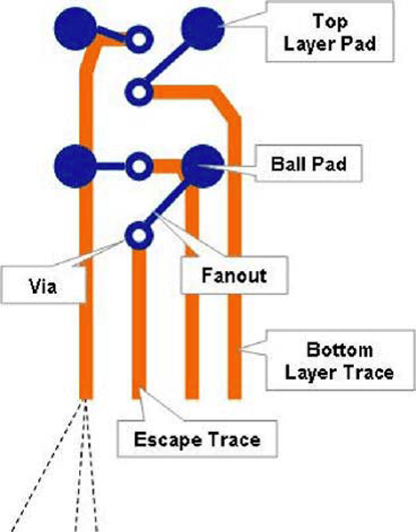
Figure 3 - BGA breakout routing features.
Fine pitch packages offer advantages and disadvantages alike. Finer pitch means that the trace and space limits will have to be adjusted down to match the BGA. Many times a design can get away with small traces underneath the BGA then fan out with a slightly larger trace width. The PCB fabrication facility will need to be aware of your design objectives and check for the smallest trace dimensions supported. Smaller traces take more time to inspect, check and align. Etching needs to be closely monitored when trace and space rules reach their lower limit. The combination of fanout traces, escape vias, and escape traces that allow routing out from under the BGA pin array to the perimeter of the device are collectively referred to as the BGA breakout (Figure 3). The fanout pattern will arrange the breakout via, layer, and stack-up to maximise the number of I/Os that can be routed.
Packaging
Lattice has created a package design for the caBGA554 and caBGA756 form factors in 0.8mm ball pitch with a new package ball break-out scheme, which allows traces to be brought from inner row balls. The package design also selectively depopulates unneeded ball positions to open up real estate for easier routing. In addition, careful assignment of signal/power/ground balls provides better skew matching, lower cross-talk among busses of high-speed signals, as well as power/ground ball assignment that allows under the DUT low inductive decoupling capacitors for supply pins.
Although this generation of SERDES-Enhanced FPGAs has achieved significant reductions in power consumption, cooling can still be an issue, especially in products which are routinely deployed in outdoor environments. For this reason, the new packaging design also maximises the number of ground vias located in close proximity to the FPGA chip itself to provide maximum conductive heat dissipation to the PCB under device. The example board shown in the top image in Figure 4 illustrates a design which takes full advantage of the benefits of ball de-population while using only two signal PCB layers (even with thru-hole vias).
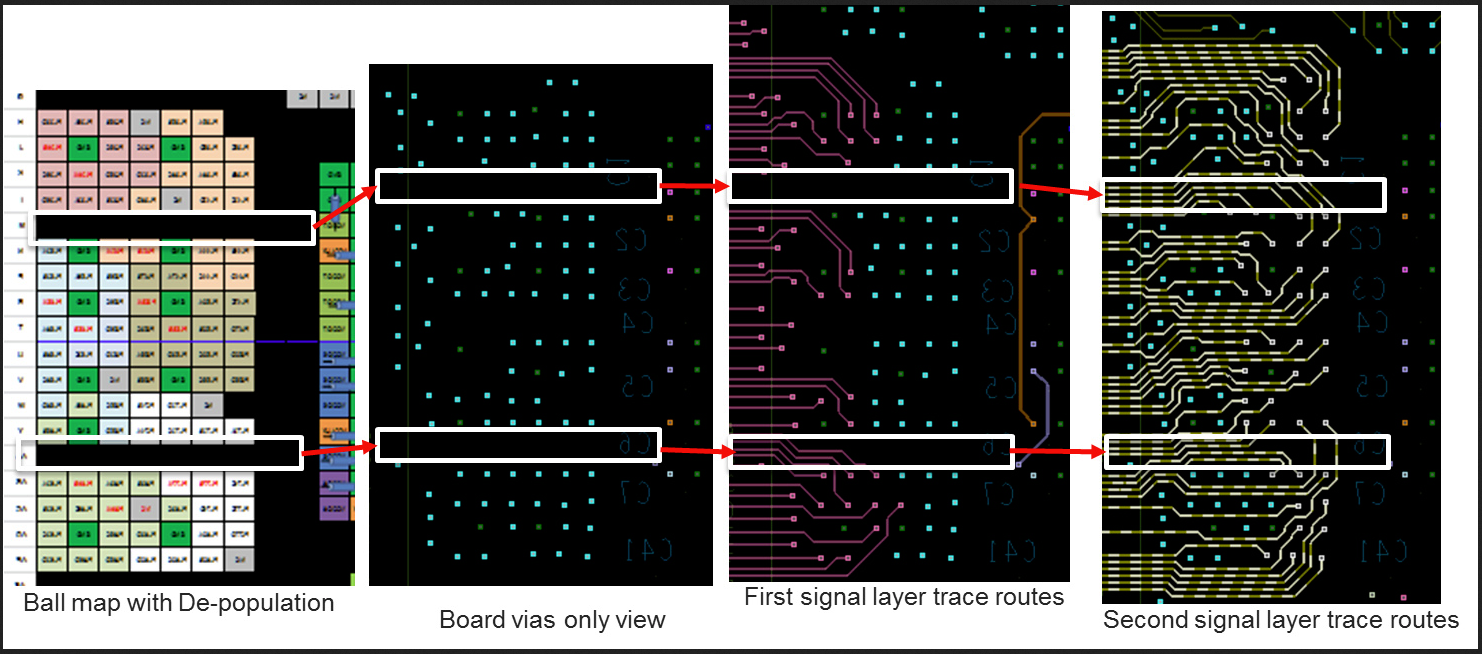
Figure 4 - Top: Depopulation of BGA balls enables simpler, cleaner trace routing using fewer PCB layers. Bottom: Unobstructed routing of SERDES signal traces allows greater control over channel characteristics which affect signal integrity.
When a row of balls on the package is de-populated, it removes vias that are needed for those balls. This creates unobstructed area on both signal routing layers, which offers more flexibility on the signal routes to break out to the edge of the package. Of greater interest however, is the routing for the SERDES signals. The de-population of selected groups of balls enables unobstructed routing of the FPGAs high speed SERDES signals. Each pair of SERDES signal traces is closely matched in terms of length and maintains accurate trace-to-trace spacing to insure stringent control over impedance. Spacing for pair to pair, and pair to FPGA signals, is also closely controlled to minimise cross talk.
By combining programmable logic with high-speed serial data transceivers, SERDES enhanced FPGAs can support a wide range of networking and system interfaces while providing programmable logic elements which can supplement and in some cases eliminate ASICs and ASSPs used in conventional designs. Their programmable capabilities help enable rapid development cycles and make it possible to create easily-upgradeable products and configurable platforms which can support multiple networking and communication standards. As with any SERDES device, they also bring several challenges to the design process, mainly in the area of packaging, PCB layout, and signal integrity. But a combination of good design practices and new packaging technologies can be used to insure SERDES-enhanced FPGAs are able to achieve their full potential.
Product Spotlight
APV1111GVY
Panasonic

Panasonic PhotoMOS® Photovoltaic MOSFET High-Power Drivers
| SKU: | |
|---|---|
| Stock: | 3490 |
| Cost: | $3.95 |
