
Let's be practical about this
From a manufacturer’s point of view, lowering cost and increasing reliability are strong factors, particularly when adding capacitive touch functionality to passive LCD displays. Hussein Isik, Technical Marketing Manager, Clocks, Watches & Graphic Drivers, for NXP Semiconductors, explores more in this ES Design magazine article.
User interfaces based on touch screens have become a must for most applications in our daily lives, whether they are for infotainment systems, equipment for personal health care, home appliances or point-of-sale machines. Influenced by smartphones and tablets, users are looking for an improved experience with their coffee machines, refrigerators, climate control units and many other devices.
Depending on the application, the requirements for the display and the touch function can vary significantly both from the cost and technology point of view. Although TFT displays with advanced capacitive touch functionality are dominating in smartphones and tablets, they might not be the most optimal solution for machines in a harsh industrial environment, or for home appliances. For instance, wireless climate control units manufactured in large volumes need a limited number of buttons, low current consumption and low cost.
Technical development around touch-screens has been driven by the portable device format, but there are many other consumer and industrial applications where capacitive touch displays are desired, but adoption has been relatively slow.
A key challenge in bringing capacitive touch displays to non-mobile applications is the required thickness of the overlay, the front glass. Unlike smartphones and tablets, the overlay of displays used in industrial and home automation products has to be thick enough for wear and tear in harsh environments. Figure 1 shows the model of a capacitive touch system: a metal pad is surrounded by a metal ring at a certain distance; a plastic overlay covers the metal pad and the surrounding metal ring.
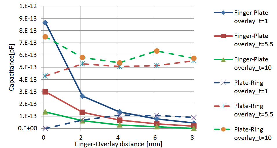
Figure 1: Capacitive change obtained with a touching finger: finger-to-pad capacitance and pad-to-metal ring capacitance
A touch sensing event was simulated with different thicknesses of overlay. Figure 1 shows the simulations results: the solid curves show the capacitance between the finger and the sensor pad, and the dashed curves show the capacitance between the pad and the surrounding metal ring. The first one is used in the self capacitance measurement method and the latter one is used in the mutual capacitance measurement method. It is clearly visible that the finger-to-pad capacitance increases exponentially as the finger comes closer to the pad, and that the pad-to-metal ring capacitance is higher when the overlay is 10mm — but with this thickness it is more or less impossible to sense the presence of the touching finger.
From the sensor IC point of view, for a certain thickness of the overlay (which is defined by the mechanical construction), highest touch sensitivity will be obtained with maximum dynamic change of capacitance during a touch.
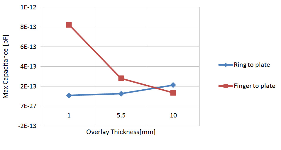
Figure 2: Maximum capacitance change at different overlay thickness
In Figure 2, the maximum capacitance change budget extracted from Figure 1 is shown for three overlay thicknesses; 1mm, 5.5mm and 10mm.
Self-capacitance measurement
From these simulation results it is obvious that for capacitive touch systems where the overlay thickness exceeds 1mm, the self-capacitance measurement method, i.e. the measurement of the finger-to-pad capacitance, is to be preferred.
Although the self-capacitance measurement method shows very high dynamic range in these simulations, the real implementation will have a smaller range due to the stray capacitance between the finger and any other neighbouring conductor rather than the sensor pad itself.
The presence of conductors reducing the self-capacitance has to be minimised not only for high sensitivity but also to reduce the sensitivity to water films or droplets on the display. In the self-capacitance measurement the increase of capacitance is a direct result of the finger bringing GND potential through the finger and creating a parallel plate capacitor, whilst in the mutual capacitance case the dielectric property of the finger will also contribute to increased capacitance between the sensor pad and the GND ring, such that the dynamic capacitance range will shrink.
Depending on the technology used for the capacitance measurement, the sampling frequency of the touch IC can vary between a few kHz and several MHz. The frame rate of the LCD driving signal of just a few hundred Hz is a potential source for interference. The interference may either be tackled by: hardware solutions of the display stack by adding a shielding layer; advanced digital filters in the touch IC; or, by using the mutual capacitance measurement method which uses an additional conductor layer for the receiver conductors.
The capacitive touch technology favoured by NXP proves to overcome the interference issue thanks to its built in digital signal processing, which efficiently prevents false triggering due to LCD signals. The auto-calibration is capable of adapting to the average capacitance level affected by the LCD noise as well presence of water films and grease on the display.
Implementations
The self-capacitance measurement method can be combined with a simple, traditional passive display to obtain a touch display. The key question is how.
Through extensive evaluation different solutions have been worked out, each suitable for different applications where production cost and complexity have been considered.
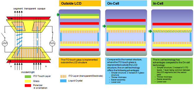
Figure 3: Touch-On-Display architectures
NXP Touch Technology supports three different Touch-On-Display architectures: add-on touch glass, where the touch layer is mounted on top of the conventional display (Figure 3a); on-cell touch, where the touch layer is positioned between the LCD glass and the polariser (Figure 3b), and in-cell touch, where the touch layer is combined with the LCD electrodes into one single layer (Figure 3c). Several demonstrators built together with major display module makers highlight the performance of NXP Touch-On-Display technology.
On-cell Touch: In this implementation, the touch pads are deposited on the display front glass sandwiched between the top polariser and the display glass. Advantages are that the whole top side of the display glass is available for touch pads and routing, and it allows sensor channels to be multiplexed for advanced functions. A disadvantage, however, is that although this implementation provides cost reduction compared to add-on touch glass, it still requires an additional step in the display process.
In-cell Touch: In this implementation, the touch pads are on the same layer as the display segments; the touch pads surround the segment electrodes. An advantage here is that as the touch pads and segments are made of the same ITO layer, in the same process step, this implementation means the touch functionality is essentially obtained for ‘free’. However since the touch and segment pattern are on the same layer, there will be some constraints on the routing, therefore the number of touch keys will be limited.
NXP offers a comprehensive portfolio of LCD drivers (available in packages and as bar die with bumps for Chip-On-Glass (COG) assembly) and capacitive touch controllers (available in packages) that allow implementation of the Touch-On-Display.
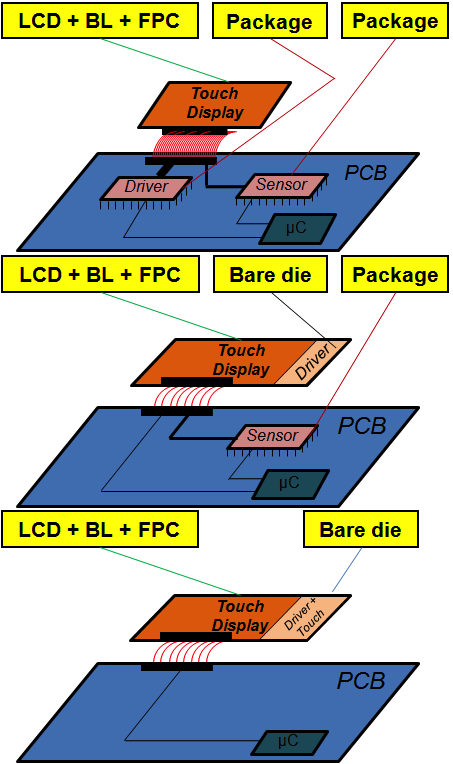
Figure 4: Driving the Touch-On-Display (Note: BL = back light, FPC = flex printed circuit connection, PCB = printed circuit board). From top to bottom: simplified PCB layout; improved modularity, ugradability and reliability; reduced assembly & testing cost; simplifies logistics.
Figure 4 shows some driving solutions. From top to bottom: simplified PCB layout; improved modularity, upgradability and reliability; reduced assembly and testing cost; simplified logistics.
The trend for touch displays is evolving from modularity towards integration, where the touch and LCD driver functions are integrated in a single chip. Assembly on the display glass will help to decrease the total test and assembly cost for the end customer and reduce the risk of yield losses. Working together with leading module makers and end customers, NXP is now developing such an IC incorporating the LCD driver and touch controller functions combined.
Product Spotlight
APV1111GVY
Panasonic

Panasonic PhotoMOS® Photovoltaic MOSFET High-Power Drivers
| SKU: | |
|---|---|
| Stock: | 3490 |
| Cost: | $3.95 |
