
Crystal clear choice for displays
MCUs with integrated drivers are providing a boost for the growing LCD market.
By Mary Tamar Tan, Applications Engineer, Microchip Technology, and Rodger Richey, Director Engineering & New Product Development, Microchip Technology.
LCDs have soared in popularity in recent years thanks to numerous advantages over other display technologies. Controlling them has also become easier because of the introduction of 8-bit MCUs with integrated LCD drivers. Prominent features of such LCD controllers include contrast control, drive waveforms, biasing methods and power modes.
These devices can directly drive segmented displays with letters, numbers, characters and icons and have been developed to meet low-cost design requirements. A good example are the PIC MCUs from Microchip, which are available in 28-, 40-, 64-, 80- and 100-pin packages and can eliminate the need for several external hardware components.
The LCD driver module generates the timing control to drive a static or multiplexed LCD panel with support for up to 64 segments multiplexed with up to four or eight commons. Figure 1 shows a typical LCD module block diagram.
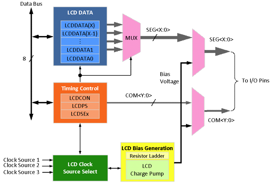
Figure 1 - Typical LCD module block diagram
The number of LCD registers varies depending on the maximum number of commons and segments that can be driven by the specific device.
Timing control block
As shown in Figure 1, the timing control block comprises the LCD control register (LCDCON), LCD phase register (LCDPS) and LCD segment enable registers (LCDSEx). The LCDCON controls the overall operation of the module. Once the module is configured, the LCDEn bit is used to enable or disable the LCD module. The LCD panel can also operate during sleep mode by clearing the SLPEn bit. The bits determine the LCD clock source and the configuration must comply with the LCD glass driving scheme.
The LCDPS configures the LCD clock source prescaler and the type of waveform. The prescaler select bits have a direct effect on the LCD frame frequency, so must be set accordingly to avoid ghosting or flickering on the display.
The LCDSEx configure the functions of the port pins. Setting the segment enable bit for a particular segment configures that pin as an LCD driver. Likewise, clearing the segment enable bit allows the pin to function as an IO port.
Data block
Like the timing control block, the data block in Figure 1 is also present in all these PIC LCD modules. It is composed of the LCDDATAx registers. After the module is initialised for the LCD panel, the individual bits of the LCDDATAx registers are cleared or set to represent a clear or dark pixel, respectively.
Specific sets of registers are used with specific segments and common signals. Each bit represents a unique combination of a specific segment connected to a specific common.
Bias generation block
There are two main methods of generating the bias voltages – resistor ladder and charge pump – both of which can be externally or internally supported by the device. The LCDref register determines whether external or internal resistor biasing is used. Setting the LCDIRE bit enables internal biasing.
When internal reference is enabled, contrast can be software controlled by configuring the LCDCST bits, which on some devices are found in a separate register. The power source for the contrast control can be selected through the LCDIRS bit. The LCDref register also determines which bias pins are used internally or externally for the different bias levels.
The LCDRL register provides control for the different ladder power modes, as well as the time interval for each power mode.
Using the charge pump method requires only the LCDreg register to be configured. When the charge pump is enabled, contrast can be controlled through the bias bits. The regulator supports either 1/3 or static bias by setting or clearing the relevant bit. The regulator also has to be provided with its own clock source through CLKSEL bits.
Frame frequency
The LCD frame frequency is the rate at which the common and segment outputs change. The clock source depends on the configured clock source select bits on the device used; PIC MCUs typically have three clock source choices for the LCD module.
The range of frame frequencies is from 25 to 250Hz with the most common being between 50 and 150Hz. Higher frequencies result in higher power consumption and ghosting while lower frequencies can cause flicker.
Clock sources
The three possible clock sources on these modules are usually fast internal RC oscillator, secondary oscillator and internal LPRC oscillator. However, for some devices the clock sources are the system clock, the timer one oscillator and the internal RC oscillator. Figure 2 shows how a clock is typically generated for the LCD peripheral.
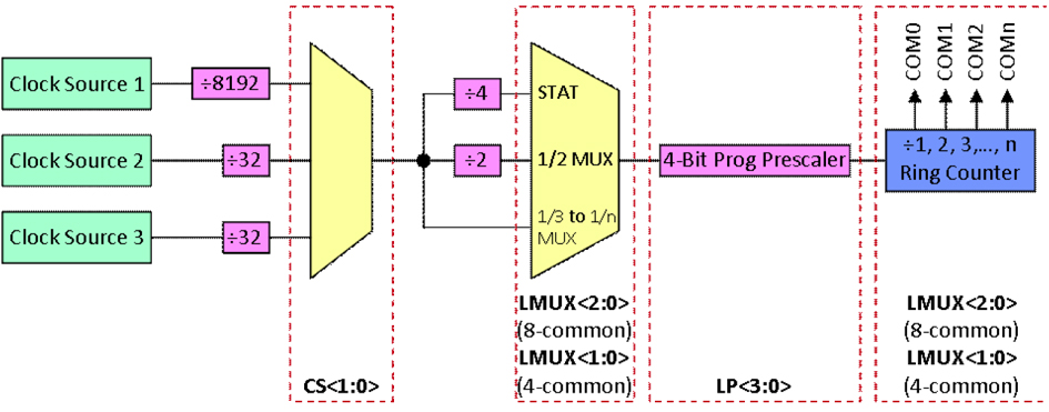
Figure 2 - LCD clock generation
For the three clock sources, a divider ratio provides about a 1kHz output. For example, if the clock source is an 8MHz FRC oscillator, it has to be divided by 8192 to produce an approximate 1kHz output. This divider is not programmable. Instead, the LCD prescaler bits of the LCDPS register are used to set the frame clock rate. These bits determine the prescaler assignment and prescaler ratio.
Typically, two of the three clock sources may be used discretely to continue running the LCD while the processor is in sleep mode.
Waveforms
An LCD can be characterised by the MUX ratio and bias, but one piece of information is still missing – drive waveforms. LCD waveforms are generated so that the net AC voltage across the dark pixel should be maximised and the net AC voltage across the clear pixel minimised. The net DC voltage across any pixel should be zero. LCDs can be driven by type A or type B waveforms.
In a type A waveform, the phase changes within each common type whereas a type B waveform’s phase changes on each frame boundary. Thus type A waveforms maintain 0VDC over a single frame and type B waveforms take two frames. Figure 3 shows both types of waveforms for 1/3 MUX and 1/3 bias.
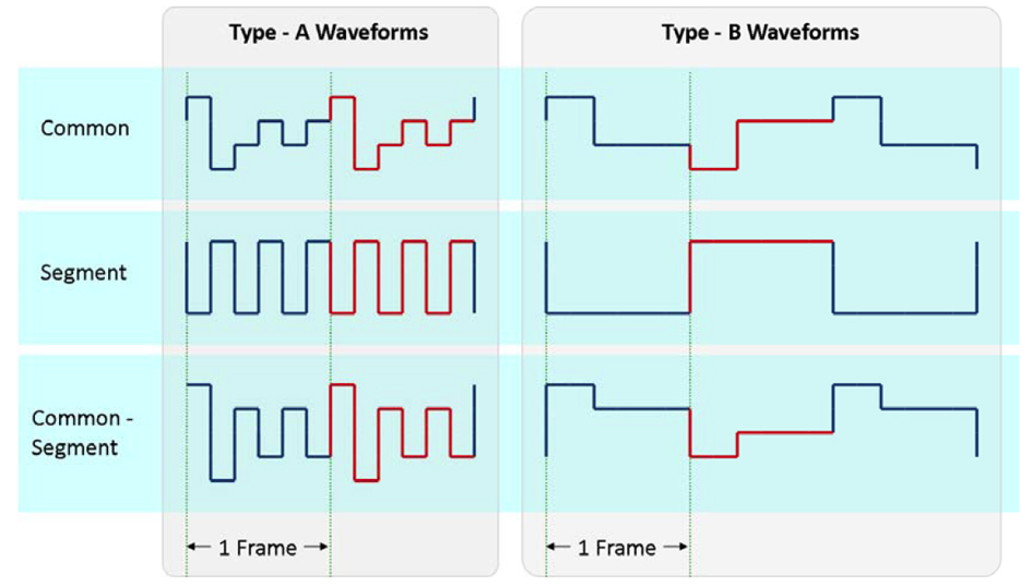
Figure 3 - Type A versus type B waveforms
The voltage applied across a particular pixel is the voltage on the COM pin minus the voltage on the SEG pin. If the resulting voltage is at or above the Von threshold then the pixel is visible. If it is at or below the Voff threshold then the pixel is not visible.
The contrast of an LCD can be determined by calculating the discrimination ratio, which is the ratio between the RMS voltage of an on-pixel and the RMS voltage of an off-pixel. Segment mapping provides a simple and organised way to determine which pixels should be on or off.
External resistor biasing
The resistor ladder method is most commonly used for higher VDD voltages. This method uses inexpensive resistors to create the multi-level LCD voltages. Regardless of the number of pixels that are energised, the current remains constant.
The resistance values are determined by the display quality and power consumption. Display quality is a function of the LCD drive waveform. Since the LCD panel is a capacitive load, the waveform is distorted due to the charging and discharging currents. This distortion can be reduced by decreasing the resistance value.
However, this change increases the power consumption due to the increased current flowing through the resistors. As the LCD panel increases in size, the resistance value must be decreased to maintain the image quality.
Sometimes adding capacitors in parallel to the resistance can reduce the distortion caused by charging and discharging currents. This effect is limited since, at some point, a large resistor and large capacitor cause a voltage level shift that negatively impacts the display quality. Adding a potentiometer allows external contrast control.
Internal resistor biasing
To avoid the trouble of adding external components and to save the use of up to three pins for voltage generation, PIC MCUs provide internal resistor biasing and internal contrast control. This mode does not use resistors but internal resistor ladders that are configured to generate the bias voltage.
The internal resistor ladder can be used to divide the LCD bias voltage to two or three equally spaced voltages that will be supplied to the LCD segment pins. To create this, the reference ladder consists of three matched resistors.
When in 1/2 bias mode, the middle resistor of the ladder is shorted out so that only two voltages are generated. This mode reduces the ladder resistance thus increasing current consumption.
Conclusion
Various MCUs with LCD controllers provide design flexibility and straightforward ways to drive the LCD glass. The internal biasing, contrast control and power-saving features in the LCD module eliminate the need for extra hardware. They let designers make the most of these features while maintaining display quality.
Product Spotlight
APV1111GVY
Panasonic

Panasonic PhotoMOS® Photovoltaic MOSFET High-Power Drivers
| SKU: | |
|---|---|
| Stock: | 3490 |
| Cost: | $3.95 |
