
Speeding IP design
Syed Zahid Ahmed, Sébastien Fuhrmann & Bertrand Granado present a cross-analysis of an ESL approach versus hand-coding in IP-based image-processing.
Some designers avoid FPGAs because of the complexity of programming – an esoteric job involving hardware description languages such as VHDL and Verilog. But the arrival of practical electronic system-level (ESL) design promises to ease the task and put FPGA programming within the grasp of more design engineers.
To test this, a cross-analysis of an ESL approach versus hand-coding was undertaken in a collaborative industrial-academic project. The aim was to provide an unbiased, independent case study, since the tools are still new and not much literature is available on the user experience. This work used the original legacy source code of the algorithms, which was written for the PC.
The design tool used was Xilinx’s Vivado Design Suite. Vivado HLS, a high-level synthesis tool, facilitates ESL design by automating the transformation of a design from C, C++ or SystemC to HDL. This was introduced to handle the increased complexity of the Xilinx 28nm Zynq-7000 All Programmable SoC, equipped with a hard ARM processor alongside the programmable logic.
In comparing hand-coded blocks of IP that were previously validated on a competitor's 40nm midrange products, with ESL programming on a Zynq SoC, the ESL results were found to rival the manual implementations in many aspects, with the notable exception of latency. Moreover, the ESL approach dramatically slashed development time.
Methodology
The Zynq-based ZedBoard was used for prototyping the experiments. Two complex IP cores were chosen from an ongoing image-processing project. These were designed in Verilog and validated on the 40nm product.
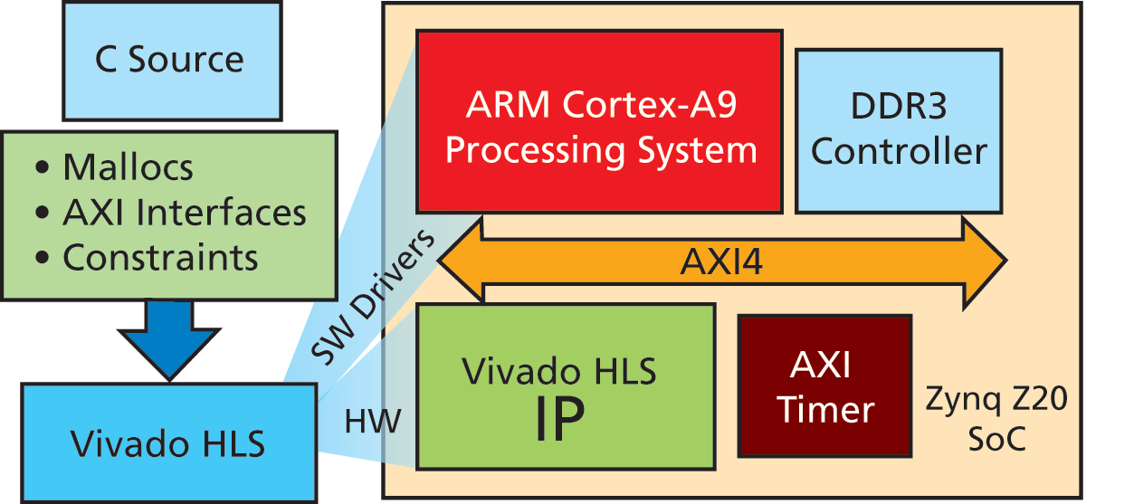
Figure 1: Test hardware system generation for the Zynq Z20 SoC
Figure 1 outlines the flow using Xilinx tools. The objective was to make few or no modifications to the original C source code apart from some tweaks for dynamic memory allocation and complex structure pointers. The AXI4 master and slave (AXI-Lite) interfaces were created on function arguments and the code processed within Vivado HLS with a single constraint made for comparison's sake involving latency. Porting the RTL code to the Xilinx environment was straightforward.
The HLS tool's built-in SystemC co-simulation feature verified the generated hardware before prototyping. Vivado HLS also generates software drivers (access functions) further accelerating the time to validate and debug the IP.
The Core-0 of the Zynq device's Cortex-A9 MPCore at 666.7MHz was used, with a DDR3 interface at 533.3MHz. An AXI4 timer took care of latency measurements. Figure 2 shows the validation flow on the FPGA prototype. The image is processed with the original C source on ARM to get the golden reference results. The same image was processed with the IP and compared to validate the results.
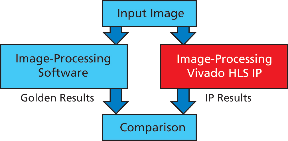
Figure 2: ESL IP validation flow on the FPGA
Experimental results
Taking a closer look at the two pieces of IP, labelled IP1 and IP2, using the HLS tools, Table 1 outlines the details of the design space explorations for IP1 in the form of steps (listed as S1, S2 and so on). The clock period, latency and power figures are reference values following a quick synthesis for the cross-analysis of multiple implementations (the actual values can vary after final implementation).
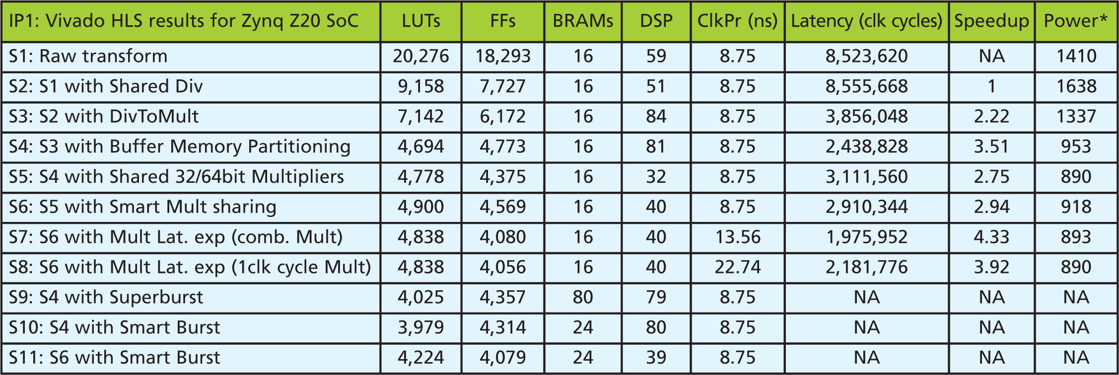
Table 1: HLS exploration results for IP1, *Power value of tool for iterations comparison, it has no units
In S1, the code was compiled with no optimisation constraints except the modifications described earlier. As seen from Table 1, the hardware uses an enormous amount of resources, the primary contributor being several division operations in the algorithm.
S2 was like S1 but with shared divider. Unfortunately, in this version of the tools it is not easy or even possible to apply custom constraints on operators directly, so the division operation was replaced by a function, and constraints can be applied. Using single, shared division hardware, as seen in Table 1, reduced lookup tables, flip-flops and other logic resources with negligible impact on latency.
In S3, the division operation was transformed into multiplication, possible because this application uses division by constant values. The approximation values were provided as function parameters via slave registers. This is why Table 1 shows improvements in performance and resources, with a slight trade-off in added DSPs due to increased multiplication operations.
S4 saw buffer memory partitioning added. The source algorithm uses multiple memory buffers in a unified block. During the initial transformation to make the algorithm HLS ready (Figure 1), that memory block became an internal on-chip memory (block RAMs). Table 1 shows the results, highlighting improvements with a slight increase in the number of BRAMs, this also yielded a decrease in logic resources.
In S5, the focus was on optimising the DSP blocks using shared resources. An analysis of the generated hardware using the Design Viewer utility cross-referenced generated hardware with the C source code. This revealed that in raw form the hardware uses 26 multiplier units of heterogeneous types, which can be classified as unsigned 16/32/64bit multiplications and 32bit signed multiplications. Table 1 shows the resulting reduction in DSP usage, albeit with some penalty in performance. To mitigate this, S6 made use of multiplier sharing. Two additional multiplier types were created: a 16bit unsigned multiplier and a 32bit unsigned multiplier with 64bit return value. This improved performance but with slightly higher DSP usage.
S7 involved two experiments for changing the multipliers’ latency. The latency was set to 0 and the corresponding combinational multiplier chosen from the library. The results show an improvement in latency. However, the design became much slower.
In S8, a single-clock-cycle multiplier was selected from the library. Table 1 shows while the latency has slightly increased, the clock period, surprisingly, has significantly increased, which may lead to slower hardware.
In S9, S10 and S11, burst access was explored. This is almost obligatory for IP based on shared-memory systems due to high latency of the bus for small or random data accesses. Even with these burst-access experiments, the software structure of the code was never modified.
Selected steps
All these steps and the results were evaluated within minutes, avoiding the lengthy implementation phase of an FPGA for only a few, final selected iterations.
The implementation statistics of the optimal hand-coded IP on the SoC were obtained by implementing its RTL using Xilinx tools. This involved using the latency measurements of previous experiments with a competitive FPGA as a reference. This highlights how HLS tools can make it easier for designers to port to multiple protocols.
Comparing results showed the quick synthesis of ESL gives a relatively good estimate compared with the actual implementation; for memory and DSP, the synthesiser can sometimes significantly change the resource count for optimisations.
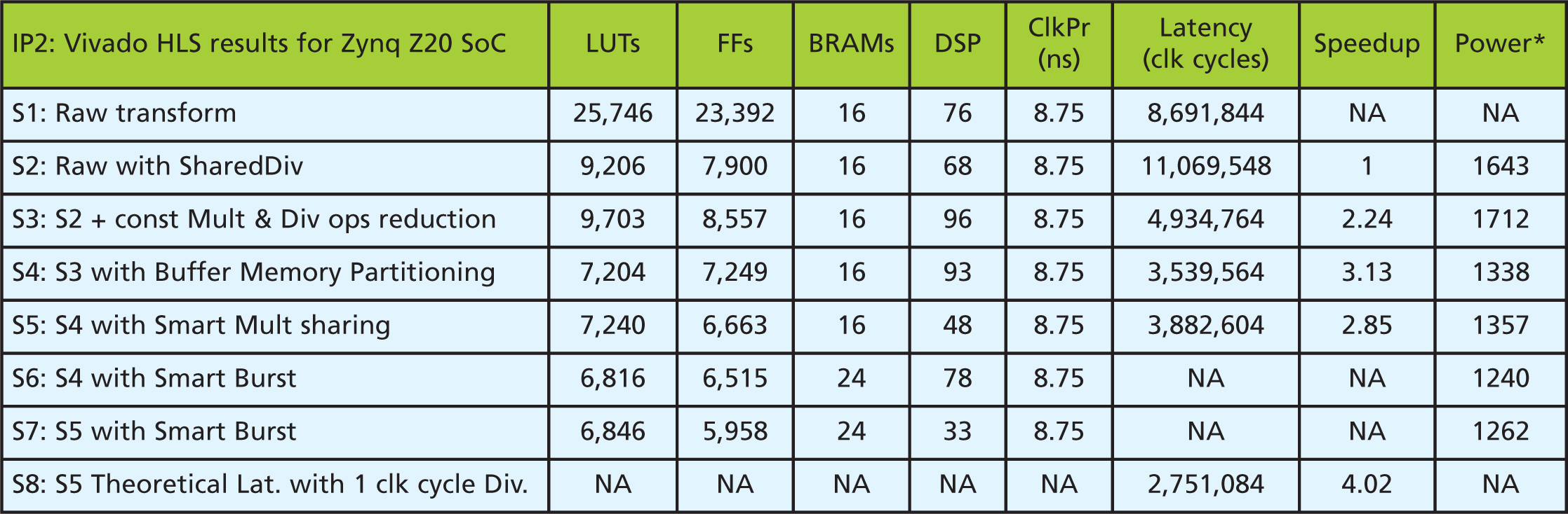
Table 2: HLS exploration results for IP2, *Power value of tool for iterations comparison, it has no units
For final implementation, timing closure can be a problem. There is a notable change in achieved frequency after FPGA implementation compared with the HLS estimate. Finally, it is surprising that even with the burst-access experiments, there is a difference in latency values from the expected HLS values and hand-coded IP. This piqued curiosity about the quality of DMA that the HLS tool generated. IP2 was similarly explored and the results can be seen in Table 2.
DMA/burst efficiency
Despite using the original source code, which was not written in an optimal manner to exploit embedded systems, the ESL tools delivered results that rivalled optimally hand-coded IP in terms of resource utilisation. The significant difference came in latency, which was far better in the hand-coded IP. Xilinx experts recommended using the external DMAs manually for optimal performance, as the master interface generated by the version of Vivado HLS used is in beta mode and will be upgraded in the future. Such factors might have caused a significant difference in latency and might be a good starting point for future experiments.
The experiments in this work revealed interesting aspects of ESL design and cleared up some misconceptions. The results obtained from ESL rivalled the optimal results in all aspects except latency. Furthermore, using accurate bit types with advanced features of the tools (instead of the generic C types used in these experiments) may further improve resources, as could partially rewriting code.
These explorations also gave an idea about productivity versus efficiency trade-offs. Figure 3 illustrates the relative development time of IP blocks. The speed up for ESL-based design is dramatic, especially for verification.
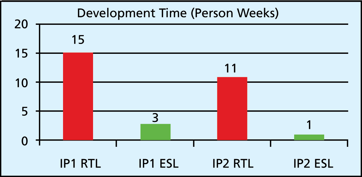
Figure 3: Hand-coded RTL versus ESL development time
Since the same people were involved in the hand-coded design and the ESL-based design, Figure 3 gives an unbiased overview of how the process plays out. Given designers were acquainted with the classical RTL method of IP design and integration, and were new to ESL tools, its likely implementation time could improve once the tools are more familiar.
Product Spotlight
APV1111GVY
Panasonic

Panasonic PhotoMOS® Photovoltaic MOSFET High-Power Drivers
| SKU: | |
|---|---|
| Stock: | 3490 |
| Cost: | $3.95 |
