
Flexibility is key
The demands placed on embedded software development systems have increased significantly in recent years. This is particularly apparent in the test and debugging sectors. Extremely high-performance, multi-core System-on-Chips (SoCs), which integrate an increasing number of functions, require radical rethinking in several aspects. By Heiko Riessland, Product Manager with PLS Programmierbare Logik & Systeme.
Not so long ago, hardware clearly dominated the value-added chain in microcontroller applications. However, at least in the high-end sector, this relationship has clearly changed in favour of software. Today, software not only forms the largest portion of the value-add, but also the development time, implementation should therefore begin as early as possible. Nowadays, with large projects this already happens long before the first real samples of new microcontrollers are available. During this phase, development systems generally serve as frontend for virtual targets, in other words for software systems with which entire SoCs or parts of them can be simulated. The advantage of this is that right from the start all persons involved in the product development can work with the same user interface and thus ultimately not only save time but also costs.
The adaptation to the simulators of different manufacturers presents an enormous challenge for development system manufacturers. After all, it is not only necessary to take the different capabilities of the simulators into consideration but also differences to the forthcoming real hardware and be able to integrate them as seamlessly as possible in the user interface. Modular development tools with strict separation of functionality and visualisation have a clear advantage, because in such cases only the affected components must be exchanged (Figure 1). The so-called Multi-Core Debug (MCD) API, which is already being used by a number of suppliers, is currently establishing itself as a standardised interface between the simulators and frontends of various manufacturers.
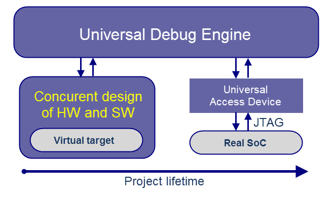
Figure 1: Supporting the same user interface for a virtual target and a real target over the course of the project
Hardware-supported simulation
Another field of application for development systems during the phase in which no real silicon is available is based on semiconductor manufacturers verifying their prototypes with hardware-supported simulation and through emulation. The Cadence Palladium series, capable of handling chip designs of up to 256 million gates, is a typical example for such hardware/software co‑verification. In this case, because the on-chip debug hardware and interfaces are also emulated, there is a possibility for development system manufacturers to also adapt and verify their tools before availability of the first devices. For this purpose, the debug hardware probe for signal conditioning and processing belonging to a professional development system merely needs to be connected to the hardware emulator. Provided a protected Virtual Private Network (VPN) connection is available for safe control via the internet, this can also be located many thousands of kilometres away.
The real-world application scenario is more complex; ultimately software must be tested, debugged and modified on the debug probe, which will later support a new microcontroller architecture. Ideally, the debug probe therefore has an Ethernet connection. This is also beneficial at the beginning of a project, when several developers must work together on one of the rare hardware prototypes.
Target interface
A high degree of flexibility of a development tool when accessing the target has now become essential. This is not only true for the software and system development phase, but also especially in view of subsequent service and maintenance tasks. Modern SoCs, such as Infineon’s AURIX (AUtomotive Realtime Integrated neXt generation architecture) family or Freescale’s Qorivva MPC57XX family, usually offer users various different levels of debug accesses and performance. In addition to the classical JTAG interface, interfaces such as DAP or cJTAG are contained on the chip, which thanks to a high serial clock usually feature the same throughput with a reduced pin requirement. Furthermore, these transmission techniques, because they are safeguarded for example by checksums, are frequently more robust than the classical JTAG. However, sometimes finding any debug access at all is welcome; out of necessity, the CAN interface is also sometimes used for transmitting debug commands, because with automotive control devices this is frequently the only one available.
Variant support
The major challenge for manufacturers of SoC development tools is ultimately to support every possible conceivable variant. This means not only modular hardware concepts, which cover the various mechanical and electrical requirements, but also the greatest possible flexibility in adapting to different protocols. The combination of these involves use of the most modern FPGA technology — for example, as used with the Universal Access Device (UAD) family from PLS Programmierbare Logik & Systeme.
A further challenge for SoC development systems is the full support of so‑called Emulation Devices. In the case of Infineon’s AURIX family and Freescale’s Qorivva MPC57XX family, besides the absolutely identical production chip and additional trigger/filter logic, these contain further on-chip emulation memory and a new innovative trace interface. The devices, which are specifically for development, are primarily intended for calibration and debugging purposes. For example, with help of the additional logic, certain cores and/or peripheral units of the multi-core SoCs can be selected for the recording of their activities. The trace information is either stored in the internal emulation memory or outputted via the trace interface. Through use of the Xilinx Aurora protocol, this offers transmission speeds in the gigabit range. However, the high frequencies which thus occur require processing close to the target. The modular construction of the PLS Universal Access Device 3+ (UAD3+) with its debug and trace pod separately connected via a fast PCI Express bus to the base unit offers a good infrastructure for an Aurora trace solution (Figure 2).
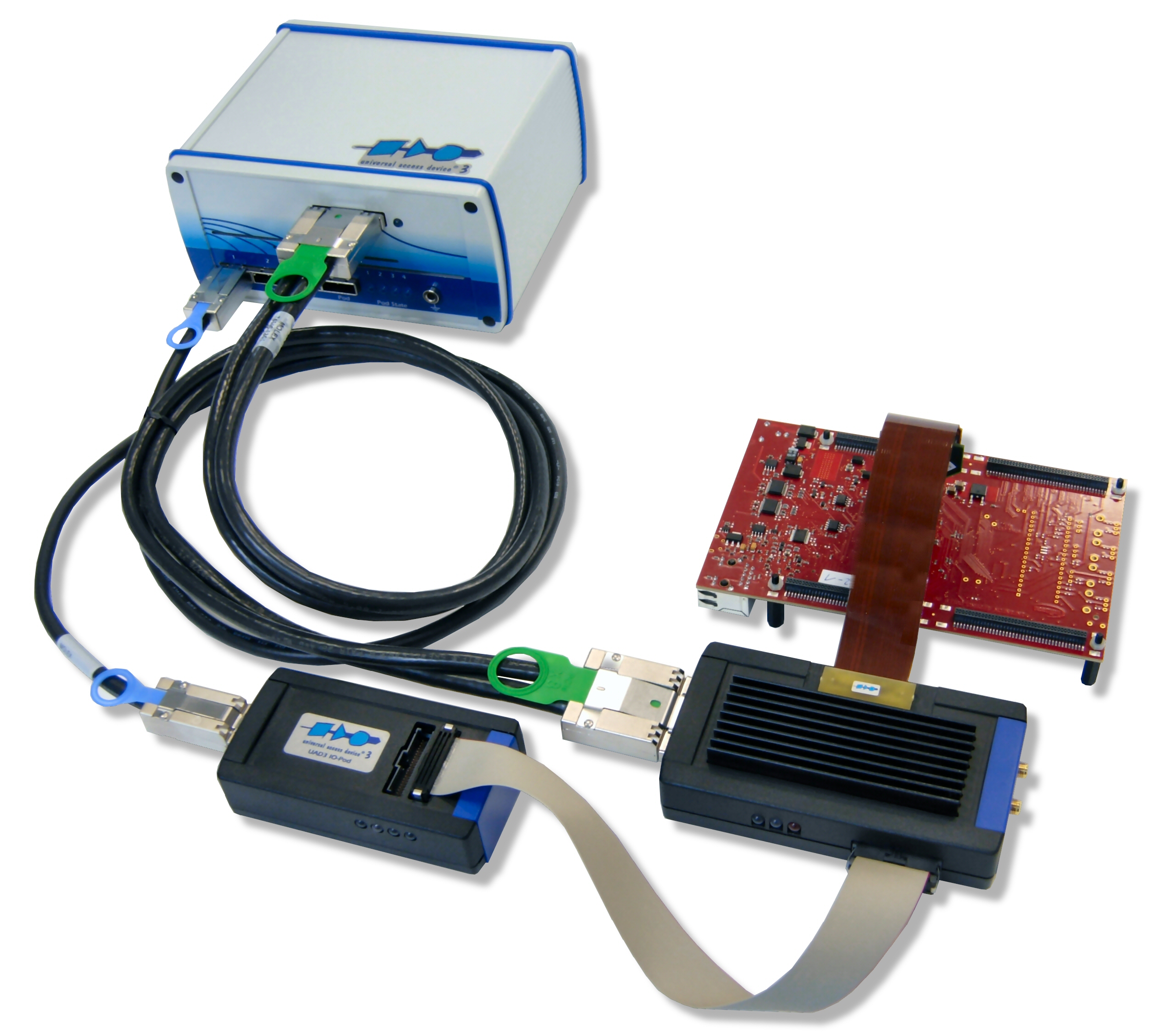
Figure 2: Serial high-speed interfaces based on the Aurora protocol with transmission speeds in the gigabit range require signal processing close to the target
In general, when using so-called Emulation Devices for trace, two different methods for different problems are apparent. Firstly, the integrated logic consisting of many hundreds of registers can be used to detect errors. Thus, the following relatively simple problem, in contrast to the past, can easily be solved: a global variable, which based on the source code is described from three functions of the application, changes so sporadically that this can not have occurred, based on value or timing, from these three functions. In this case, with help from the trigger logic and trace logic of the Emulation Devices, all write accesses to this variable which don’t arise from these functions can be recorded. This can also occur over a longer period of time, whereby after such an access the system can be stopped for evaluation. However, for effective use of the Emulation Devices, special tools are necessary that are able to configure the many hundreds of registers of the trigger logic and filter logic at a higher level of abstraction. For example, the Universal Emulation Configurator (UEC) from PLS allows the schematic definition of trace and measurement tasks on the basis of a state machine model with signals, states and actions. This approach also supports complex error conditions.
With the second trace method, a large amount of data outputted via the Aurora GigaBit Trace (AGBT) is statistically evaluated and used for system level debugging — for example, for code coverage analysis or performance profiling. The prerequisite for this is a development tool with a sophisticated trace framework, which can not only process large amounts of data from various sources, but also offer extensive graphical presentation possibilities for effective evaluation of the data.
Debugging under field conditions
A further challenge for manufacturers of development tools for complex SoCs is that during the evaluation phase of a new application, unfortunately, not enough thought is given to what happens with the embedded application once it has left the developer’s desk. In both automotive and industrial environments, in many cases debugging under field conditions is also necessary.
Some general points must be observed; signal conditioning and preprocessing close to the debug interface may often be necessary in order to support a sufficient distance between the target and PC in use, whereby it is absolutely necessary to distinguish between the target connectors or adapters and the actual probe. In order to go beyond the usual and, for a laboratory bench mostly sufficient, cable length of 20 to 25cm, there are several options. For example, special JTAG extenders from PLS, which provide conversion of differential signals close to the target; allow a cable length of up to two metres to the probe. With the debug pods of the UAD3+ connected via PCI Express, cable lengths of up to five metres are permitted. In conjunction with an Ethernet connection to the probe, debugging directly within the vehicle or under industrial field conditions is also possible. Furthermore, in order to enable in-the-field operation an additional input voltage range should be available for powering the probe.
.jpg)
Figure 3: A size comparison between a target adapter and a target adapter with electrical isolation (right)
A further challenge that should not be underestimated, especially with controls for electric motors or inverters, is represented by potential differences between the control electronics and parts under high voltage. For the signals requiring processing, the inputs of the debug probe must be as sensitive as possible, but at the same time they should also be robust against overvoltages. Here, adapters with electrical isolation are offered that combine sufficient speed and electric strength, which due to their small dimensions are almost completely insensitivity to magnetic fields. Such adapters, in combination with the Universal Access Devices 2pro (UAD2pro) and UAD3+ from PLS, are now available for numerous debug interfaces (Figure 3).
It’s a fact that much higher demands are now placed on development systems for testing and debugging embedded software; much more than was evident only a few years ago. This is due not only to the significantly increased complexity of SoCs, but also the fact that developments tools are increasingly employed outside the usual laboratory conditions, which presents entirely new challenges to the hardware and software components. Making savings in the wrong place can sometimes mean paying a high price over the entire embedded product lifecycle.
Product Spotlight
APV1111GVY
Panasonic

Panasonic PhotoMOS® Photovoltaic MOSFET High-Power Drivers
| SKU: | |
|---|---|
| Stock: | 3490 |
| Cost: | $3.95 |
