
Middleware covers the middle ground
IP developed to bridge the gap between software and hardware design handles FPGA partial reconfiguration automatically, enabling a dynamically reallocating processing platform. By Dirk van den Heuvel, Hardware Architect, TOPIC Embedded Systems, and René Zenden, System Architect, TOPIC Embedded Systems.
Over the last three decades, FPGA technology has evolved from primarily programmable logic arrays with a few registers into the advanced, integrated system devices we know today. A little over a decade ago, vendors first began offering 8-, 16- and 32-bit soft processors on their FPGAs to achieve greater degrees of integration and functionality between processing and programmable logic. They then started implementing hardened versions of these processors, offering customers even more system benefits.
Today, devices like Xilinx’s Zynq-7000 All Programmable SoC represent the state of the art among such devices. With its ARM dual-core Cortex-A9 MPCore processing system, FPGA fabric and peripherals all on a single device, the Zynq SoC has moved the hardware and software worlds closer together than ever before, enabling new degrees of system-level integration and functionality.
But this tighter integration has, as a consequence, blurred the boundaries between software and hardware design, as it introduces FPGA design in the software domain and application software development in the FPGA domain.
TOPIC Embedded Systems has developed an IP block intended to significantly reduce the development time and costs of creating systems on the Zynq SoC. The Dyplo system’s middleware functionality tackles the gap between hardware and software design, and provides a means to enable a fully software-driven development flow. It uses automatic partial reconfiguration, an advanced design technique in which the FPGA layout can change its hardware configuration on the fly to best optimise performance for a given task. This approach is used to link scalable data streams via standard AXI interfaces between individual FPGA processes and processor-executed software processes.
Concept
The concept behind Dyplo can best be explained from a development perspective. At the start of a design project engineers first capture the design requirements. This is often in abstract terms and so changes in requirements are relatively painless in this phase.The next step translates the requirements into a design specification; a blueprint of the implementation architecture. In this architectural-definition step, functions can be partitioned between hardware and software, and timing goals set. In many cases there are multiple architectures possible, but budgets and time often limit the exploration to a small number of implementation architectures. Requirement changes can at this level start to become more expensive.
Following the architectural definition, design of the various functions begins. This is typically the step in the design process where missed details are discovered, justifying an implementation swap from hardware to software or vice versa. Usually such a swap will cause pain in the development effort, such as solving problems in domains where they should not be; disruptive control functionality in DSP-type data flows, for example. Such scenarios are very common, as the customer’s insight evolves over time in tandem with their understanding of the complexities of the design. Therefore, designers need a mechanism to easily move functionality between hardware and software.
Figure 1 illustrates a common arbitrary scheduling scenario in which processes are mapped on FPGA hardware and in software without a common approach (a). A more structured and predictable infrastructure between software and hardware is necessary. Dyplo implements this infrastructure (b).
 where hardware designers enter HDL into Zynq SOC’s logic blocks and software designers enter software on the processor.jpg)
Figure 1: Instead of having two separate processes (a) where hardware designers enter HDL into Zynq SOC’s logic blocks and software designers enter software on the processor, Dyplo creates a single point of code entry for both hardware and software functionality (b). This facilitates system-level co-design and verification in a Linux environment.
Dyplo provides users with streaming data interfaces between hardware and software processes. Process communication can be between software processes individually, hardware processes individually and combined hardware/software processes. With Dyplo, hardware processes can be defined in reconfigurable partitions. To enable a given hardware function, it is activated on one of those reconfigurable partitions. Once initialised, the input and output streams to and from that partition connect those streams to your software processes or other hardware processes. Apart from data stream synchronisation, it is also possible to synchronise processes on events such as framing boundaries, discrete sample moments and software task alignments.
The number of software processes is limited to the operating system being targeting and how the process communication is organised. The number of hardware processes is limited to the number of reconfigurable partitions reserved on the FPGA. The amount, size and locations of the reconfigurable partitions can be user configurable or automatically chosen.
Dyplo handles the process communication and synchronisation by means of a hardware and software communication backplane with scalable performance. For example, the default configuration allows four HDMI video streams to be active simultaneously while maintaining full data-exchange capabilities with the processor.
Infrastructure
The Dyplo infrastructure realises the functionality mapped on the reconfigurable partitions as well as a full Linux distribution, using a graphical tool flow that is compatible with the standard Vivado Design Suite project flow.
On the fly, the software and hardware process execution can be stopped, the functionality of the processes replaced and execution continued. In the case of software processes, this is trivial and designers can augment their code limited only by the abilities of the operating system chosen for the project. In the case of hardware processes, the partial reconfiguration procedures are executed to replace functionality of a part of the FPGA without compromising the execution of other programmable logic or of the external physical interfaces. The correct loading and verification of the logic modules occur automatically.
In this way, Dyplo integrates hardware process execution in a software environment while making the benefits of FPGA functionality seamlessly available to software programmers. The Zynq SoC alone brings a lot of benefits in terms of hardware system-level integration. All features are available for an all-software programmable platform. However, from an application point of view, a middleware layer is required to benefit from this architecture, made possible by Dyplo.
Extensive use is made of the partial reconfiguration capabilities of the FPGA. For a designer, partial reconfiguration is not a trivial task due to the complexities of loading and managing partial bitstream files and the need to maintain consistency in a design when changing parts of the FPGA. Also, the placement and routing with respect to physical dependencies require fairly advanced experience in FPGA design..
Dyplo provides out-of-the-box, integrated partial reconfiguration support. Default areas for partially reconfigurable partitions are reserved based on configuration parameters such as the number of required partitions and the logic complexity of a given reconfigurable partition. By providing the HDL descriptions of functionality of such a reconfigurable block, Dyplo automatically generates the partial bit files.
As part of a software application, the reconfigurable block gets its function by issuing a simple software instruction. Dyplo takes care of all required steps to execute the hardware function, such as graceful termination of the currently running function, programming of the new functionality, connection of data streams, configuration of the block and activation of the function.
Hard benefits
As the Dyplo framework handles integration with the processor environment while minimising the need to support low-level software, the vast majority of design effort can now be spent on the implementation of functionality. The benefits of FPGA technology are especially effective with high-speed interface design, high-data-bandwidth circuits and accelerated algorithmic processing. Interface and high-bandwidth circuit design will always require manual labor and technical insight into the technology benefits of FPGA devices. In the case of accelerated algorithmic processing, system-level synthesis tools like Vivado HLS will start playing an increasingly important role. However, even the use of high-level synthesis requires some design experience to judge the implementation effectiveness.
The Dyplo infrastructure makes it easier to embed algorithmic processing blocks, providing a high-speed configurable interprocess communication network among these algorithmic processing blocks, I/O blocks and the processor-implemented functions. The processing blocks are architected so as to make them suitable for partial reconfiguration. There are clear interfaces to the blocks: AXI4-compliant streaming data interfaces with the high-speed interconnection fabric and a simplified processor bus interface directly with the processing system. Links to other FPGA logic or to the device I/O are implemented using a dedicated, scalable interface. Dyplo has sufficient performance to support, for instance, multiple 1080p input and output video streams and to attach them with little configuration effort.
Using Dyplo, design teams can streamline their HDL coding effort significantly, but even more benefits can be found on the software side of system design. The Dyplo method allows teams to isolate software functions for hardware implementation, prototype them in software and then transform them into hardware, maintaining the same interface behaviour. Conversely, different functions can share the same FPGA fabric under software control. This approach, which is comparable to software thread behaviour, can reduce FPGA cost, as smaller devices are required.
From a software system perspective, the coherence between the individual processes and their connectivity can be considered as a process network with both data and event synchronisation mechanisms. Figure 2 illustrates how software and hardware processes are linked with the Dyplo infrastructure.
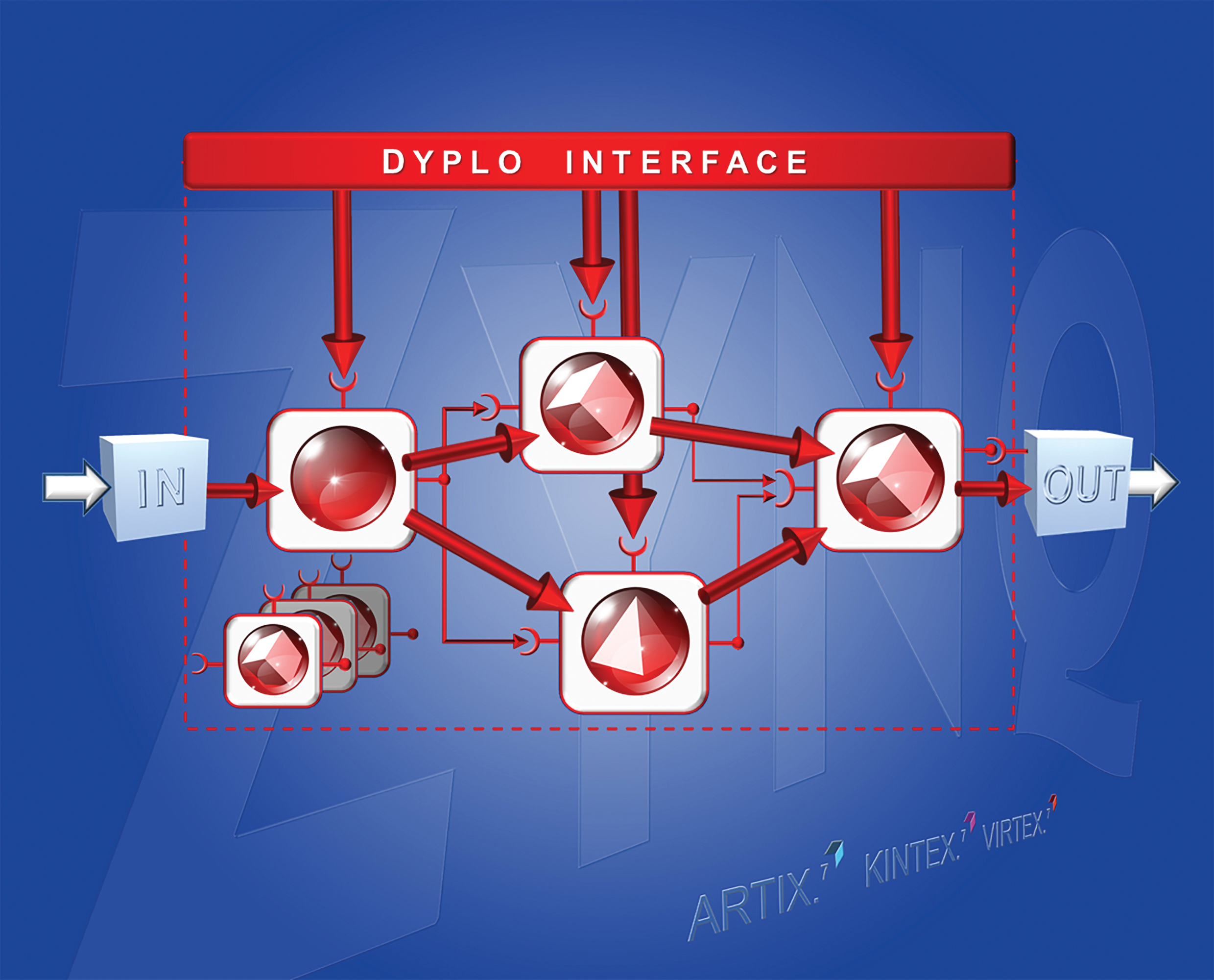
Figure 2: The balls, cubes and pyramids represent functions or processes that can run on FPGA hardware or in software. The processes are encapsulated in a Dyplo canvas (the squares around the figures). The arrows represent data flowing from the input through the different processes to the output. The Dyplo interface manages this whole process.
This method also allows dynamic performance scaling, as multiple instances of the same functionality are possible depending on the system execution context. The result is flexibility of GPU-accelerated process execution, but with much more performance. The technique also makes FPGAs much more accessible to software engineers, as the interface protocol is straightforward and the complexities of the design can be separated into blocks of manageable complexity. More importantly, Dyplo matches perfectly with Vivado HLS, because the interfaces are compatible, fitting nicely in a software-driven development flow.
As the data streamed to or received from an HDL module can be stored in files that the HDL testbench can use for pattern generation, verification teams can focus solely on the required functionality.
Test and debug
Complex system integration can be quite time-consuming and verification even more difficult. The infrastructure was developed knowing that test and integration takes a large portion of the development time and are the least appealing part of a development cycle. As it is being configured, the basic Dyplo environment generates testbench templates for verification. For example, for every reconfigurable block in the infrastructure, the Dyplo environment generates a functional testbench template, implementing streaming inputs and outputs from files or regular expressions as well as bus-functional models that implement the CPU interface (see Figure 3). This allows designers to adopt a test-driven design methodology. The infrastructure allows design teams to single-step a design to find issues and perform backplane performance analyses so as to visualize all relevant state information on the fabric. The concept is so flexible that stopping the HDL logic of the Dyplo infrastructure automatically will synchronise software execution. This functionality is critical to identifying and solving interface and dynamic problems.
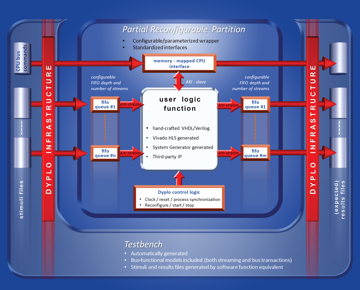
Figure 3: A functional testbench template implements streaming inputs and outputs while a bus-functional model implements the CPU interface.
The Zynq SoC, as a multiprocessor platform with embedded FPGA technology, increases the effectiveness of embedded system design significantly. But the challenge for many design teams is how to best take advantage of the Zynq SoC’s rich feature set given the expertise of designers in either software or hardware engineering.
Using reconfigurability to its full extent makes reuse of FPGA fabric very simple from a software application perspective and contributes to a lower product cost. Automating many of the low-level design, integration and test tasks at the FPGA-design and software-design levels streamlines the design process. In short, the productivity, flexibility and performance optimisation enabled by the Dyplo middleware system allows design teams to get the most out of the Zynq SoC and get innovative system designs to market faster. A beta version was released on Dec. 1, 2013 for a restricted group of customers; users who wish to participate in this program can contact TOPIC. The commercial version will be launched on March 1, 2014.
Product Spotlight
APV1111GVY
Panasonic

Panasonic PhotoMOS® Photovoltaic MOSFET High-Power Drivers
| SKU: | |
|---|---|
| Stock: | 3490 |
| Cost: | $3.95 |
