
Chip-to-chip at the speed of light
As data centres and data farms continue to expand and grow, better solutions are required for system architectures that allow faster communication and more efficient operation. The physical limits imposed by copper PCB traces are being reached - communication over copper is limited to around 10GBps, and at high speeds losses limit the distances to a few inches.
Since modern data centres require the fastest possible communication, copper effectively limits system architectures by requiring that processors be placed directly next to memory chips, for example.
One solution that’s becoming popular in data centres is moving high-speed signals from the electrical domain to the optical domain in order to take advantage of the properties of fibre optic technology. While fibre optics are well known and commonplace in long distance communications applications, modules have historically been too expensive, bulky and power hungry for point to point communications over relatively short distances. However, improvements in technology have made it feasible to install point-to-point links on PCBs, jumping over or ‘flying over’ from one chip to another, often from a processor directly to a memory chip.
Compared to copper, fibre optic links can transmit signals much, much faster - with current technology, tens of Gbps, but future technologies could see this accelerated to 1Tbps or even beyond. Although there are still some losses, they are very minimal compared to copper wires, boosting signal integrity so fast transmissions can be sent efficiently from one end of the board to another. On the other hand, since optical connections require additional components to convert signals between the electrical and optical domains at either end of the link, there is an overhead in terms of cost. Designers also have to contend with increased design and manufacturing complexity. For high end, high speed data centre applications though, this trade off is well worth it.
Real world implementations of chip-to-chip fibre optics rely on optical transceiver modules, which take electrical signals and convert them to optical signals by flashing a laser LED on and off at one end of the plastic cable, with a companion module at the other end of the cable. The transceivers are connected by single- or multi-mode plastic fibre with the appropriate connectors mounted on each end. Thankfully for those unfamiliar with photonic system design, there are cable assemblies available that include optical transceiver modules inside the connectors at each end of a convenient cable assembly.
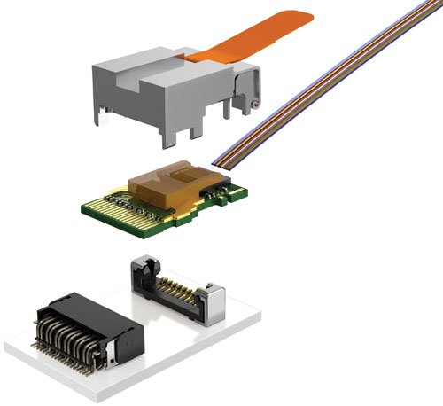
One of the most advanced chip-to-chip optical solutions on the market comes from Samtec: the FireFly Micro Flyover System. FireFly enables data rates up to 28Gbps using OM3 multi-mode fibre and an 850nm VCSEL (Vertical Cavity Surface Emitting Laser) array for 4 and 12 bidirectional channels. Chip inputs and outputs are simply routed to a connector mounted on the board next to the chip, which connects with the Firefly cable assembly. Samtec’s connectors do all the work; each one is an end-to-end electro-optical system in its own right, complete with heat sink. All data centre and HPC protocols are supported, including Ethernet, InifiniBand and Fibre Channel, and extended temperature versions (-40°C to 85°C) are available too.
Using a flyover system like FireFly frees up space on the board, despite the footprint of additional connectors, as the space that long copper traces would have taken up is gained. Components can be placed more densely under the flyover and routing is much simpler than for high speed signalling over copper. Lossy board materials and other signal degrading components are avoided, vastly improving electrical performance. And compared to alternative solutions, Samtec’s FireFly system is the smallest, most power efficient, lowest cost and easiest to use that we’ve seen.
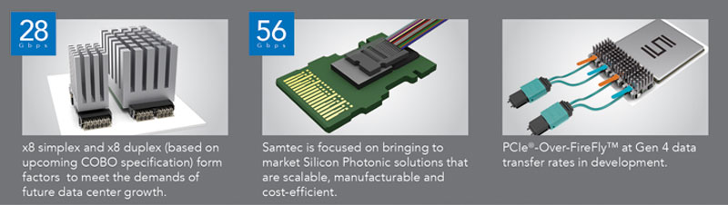
The data centres of the future will employ chip to chip fibre optic connections as standard, getting signals where they need to be as fast as possible while using less power and emitting less heat. Unconstrained by the limits of copper, new types of architectures will be made possible – memory will be placed further from processors, even on a separate board so more memory chips can be used. Layouts can be arranged to cool processors and memory chips more easily and effectively if they don’t have to be so close together. And as the technology continues to evolve, faster speeds will be possible. The next milestone on Samtec’s technology roadmap is a 56Gbps version of FireFly, which will use PAM4 (4-level pulse amplitude modulation) as a way to pack more data bits into the same amount of time for faster signals. Samtec has this technology already well underway in its development facilities.
Click here for more information.
Product Spotlight
APV1111GVY
Panasonic

Panasonic PhotoMOS® Photovoltaic MOSFET High-Power Drivers
| SKU: | |
|---|---|
| Stock: | 3490 |
| Cost: | $3.95 |
