
Stretching thin crystals for better solar cells
Stanford researchers have developed a semiconductor crystal with a variable band gap which means, among other potential uses, this variable semiconductor could lead to solar cells that absorb more energy from the sun by being sensitive to a broader spectrum of light.
Do you know how many kinds of crystals nature produces? There’s salt, snowflakes, and quartz – just to name a few. As many of you tech-savvy folks probably know, there’s plenty of crystals used in electronics. Electronics are based on a family of crystals known as semiconductors (typically silicon).
Well, Standford researchers figured out that stretching these crystals could actually produce more efficient solar cells.
To make semiconductors functional, engineers tweak their crystalline lattice in subtle ways to start and stop the flow of electrons. Semiconductor engineers must know exactly how much energy it takes to move electrons in a crystal lattice, a form of energy measure called the band gap.
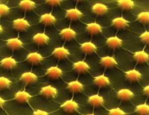
Ultra thin layer of semiconductor material stretched over the peaks and valleys of part of a device the size of a pinkie nail. (Image via Hong Li, Stanford Engineering)
Semiconductor materials like silicon, gallium arsenide and germanium each have a band gap unique to their crystalline lattice. This energy measure helps determine which material is best for which electronic task, according to Stanford University.
Well, now Stanford researchers have developed a semiconductor crystal with a variable band gap which means, among other potential uses, this variable semiconductor could lead to solar cells that absorb more energy from the sun by being sensitive to a broader spectrum of light.
The material that the researchers are working with isn’t new: Molybdenum disulfide, or MoS2, is a rocky crystal, like quartz, that is refined for use as a catalyst and a lubricant, but Xiaolin Zheng and Hari Manoharan from Stanford proved that MoS2 actually has useful and unique electronic properties that derive from how this crystal forms its lattice.
The material is what scientists refer to as a monolayer and the rock found in nature is made up of many of these monolayers stacked like a ream of paper. Each MoS2 monolayer has semiconductor potential.
“From a mechanical engineering standpoint, monolayer MoS2 is fascinating because its lattice can be greatly stretched without breaking,” Zheng said.
“With a single, atomically thin semiconductor material we can get a wide range of band gaps,” Manoharan said. Another great aspect of the material is that it is pretty cost-effective and inexpensive to make from an industrial standpoint.
The team suggests potential applications in sensing, solar power, as well as a variety of other electronics.
Product Spotlight
APV1111GVY
Panasonic

Panasonic PhotoMOS® Photovoltaic MOSFET High-Power Drivers
| SKU: | |
|---|---|
| Stock: | 3490 |
| Cost: | $3.95 |
