
Imec improves reliability of deeply-scaled CMOS logic devices
At this week’s IEEE International Electron Devices Meeting 2015, nano-electronics research centerimec presented breakthrough results to increase performance and improve reliability of deeply scaled silicon CMOS logic devices.
Continued transistor scaling has resulted in increased transistor performance and transistor densities for the last 50 years. With transistor scaling reaching the critical limits of atomic dimensions,imec’s R&D programme on advanced logic scaling targets the new and mounting challenges for performance, power, cost and density scaling to future process technologies. Imec is looking into extending silicon CMOS technology by tackling the detrimental impact of parasitics on device performance and reliability, and by introducing novel architectures such as gate-all-around nanowires, that are considered to improve short channel control.
One of the achievements is a record low contact resistivity of 1.5 Ωcm2 for n-Si that was realised by combing dynamic surface anneal (DSA) to enhance P activation in highly-doped Si:P, with Ge pre-amorphisation and Ti silicidation. Imec also presented a decreased access resistance in NMOS Si bulk finFETs by applying extension doping by phosphorus doped silicate glass (PSG) to achieve damage free and uniform sidewall doping of the fin. Finally, imec introduced junction-less high-k metal-gate-all-around nanowires to improve on- and off-state hot carrier reliability.
“I am extremely proud with the record number of 23 papers that we present at this year’s IEDM2015,” stated Luc Van den hove, President and CEO, imec. “Our presence rewards and confirms our leading position in advanced semiconductor R&D. As much as 10 of the presented papers concerned the different aspects of our advanced logic programme. Next to our research efforts to extend silicon CMOS technology into 7nm technology node and beyond. We are looking into beyond silicon CMOS, integrating high mobility materials to increase the channel mobility, and explore new concepts beyond silicon such as spintronics and 2D materials.”
Imec’s research into advanced logic scaling is performed in cooperation with imec’s key partners in its core CMOS programmes including GlobalFoundries, Intel, Micron, Panasonic, Qualcomm, Samsung, SK Hynix, Sony and TSMC.
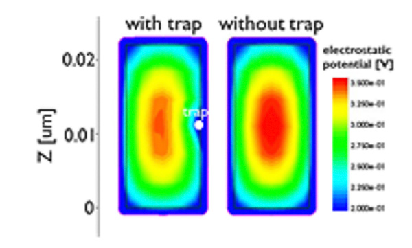
Cross-section of JL nanowires with or without an acceptor type interface, cut along the middle of the gate. The electrostatic potential is asymmetric when a trap is introduced; the squeezed channel improves the electrostatics and the subthreshold slope.
Product Spotlight
APV1111GVY
Panasonic

Panasonic PhotoMOS® Photovoltaic MOSFET High-Power Drivers
| SKU: | |
|---|---|
| Stock: | 3490 |
| Cost: | $3.95 |
